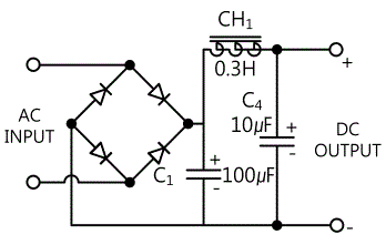
PART10Power Supply Circuit
Experiment Purpose
- 1.Investigate characteristics of power supply circuit using bridge rectifier.
- 2.Investigate characteristics of voltage regulator through experiment.
- 3.Investigate characteristics of transistor of variable voltage regulator and power supply circuit using OP Amp method through experiment
Experiment 1 :Bridge Rectifier and Smoothing Circuit
Theory
Half-Wave Rectifier
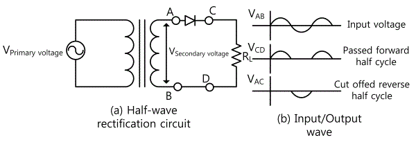
When changing AC to DC, diode is used and this is called rectifier and the process is called rectification. The most basic way of rectification is the half-wave rectifying circuit in fig. 10-2. When the secondary voltage of transformer is + half cycle(VAB is +), Diode D1 becomes forward bias, and it indicates very low resistance value to the voltage source so most of the secondary voltage is shown at the both ends of load resistance RL. Forward biased diode shows forward voltage drop of 0.5~1.0V in case of silicon, and of 0.2~0.6V in case of germanium. The voltage drop is mostly ignored to simplify the circuit interpretation, and especially when the supplied voltage is high, the forward voltage drop of the diode becomes very small proportion to the output voltage.
Fig. 10-2 (b) explains the operation of half-wave rectifier. Here, note that the output VCD becomes 0 when the transformer voltage VAB is minus(-). This is becomes the diode becomes reverse bias(the positive polarity is added to the negative polarity). Ideally, this is same as the open circuit. The average DC voltage(Vdc) is same as 0.318 times of the maximum value(0.318 = 1/π). Most voltmeters indicate average value so it indicates 0.318 of the maximum voltage in case of half-wave circuit. However, to calculate the power, effective value should be used. The effective voltage of half-wave rectification circuit is 0.5 times of the maximum value.
In case of half-wave,


These two way of voltage indication can be confusing. Fortunately, in DC we normally use, the average value and effective value are almost same so there is no need to worry. The current earned by dividing the average voltage of load by the load resistance is called the average voltage I0.

In case of forward bias, the voltage drop is very small. However, In case of reverse bias, the maximum input voltage is appeared as the voltage drop at both ends of the diode. This is called peak reverse voltage(PRV). All diodes have maximum permitted PRV which cannot be exceeded, and if it is exceeded, the element will be burnt. In case of the reverse biased diode, the diode voltage diode VAC of the diode in fig. 10-2(b) follows VAB so the diode has very big resistance value. Also, note that when D1 is forward biased, the voltage drop(VAC) is not “0” and it has small defined value. This is the forward voltage drop of diode, which is smaller than 1V.
Full-Wave Rectifier
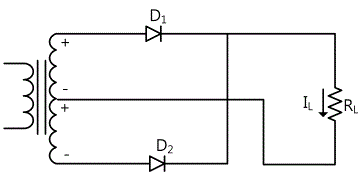
Generally, more useful and effective way to transform AC to DC is using both + and - range of AC input signal. There are two circuits used for this purpose, and one of them is indicated in fig. 10-3. This method uses whole input wave form as DC input and is known as full-wave rectification.
The center-tap rectifier in fig. 10-3 uses secondary coil that has the center-tap. If the polarity of voltage is same as in the fig., the positive electrode has + polarity to the negative electrode, so D1 is forward biased and conducted, while D2 is reverse biased and non-conducted. Therefore, only D1 produces electric current to the load.
In the next half cycle of AC, the polarity of the secondary voltage of transformer is reversed so the situation becomes the opposite. Therefore, D1 is reverse biased, D2 is forward biased and D2 produces electric current to the load. Each diode is conducted only during the half cycle(half cycle in turn) so the load current which is double of half-wave rectification current is produced.
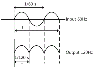
The output wave form of this is indicated in fig. 10-3. Here, note that the frequency is actually doubled at the output. This is because the period T of the output wave form is 1/2 of the AC input signal. Remember that the frequency is the reciprocal of the cycle (f = 1/T).
In most DC power supplies, the center-tap circuit was the most universal full-wave rectification circuit until the tube diode was replaced with silicon diode. However, with the advent of silicon diode which is cheap, credible and small, bridge circuit became the most universal form.
That is because the size of transformer needed to gain the output which is as big as that of center-tap circuit can be reduced. In the center-tap circuit, during each half cycle of + and -, the electric current flows in turn at the half of secondary part of the transformer.
Bridge Rectifier
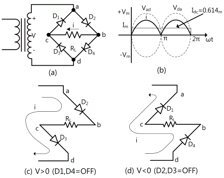
Compared to half-wave rectifier, the bridge rectifier in fig. 10-5 can flow double DC load current with same transformer voltage. In the half cycle in which the transformer voltage V=Vac is +, the electric current flows in the direction indicated in fig. 10-5(c), and in the half cycle in which V is -, it flows in the direction indicated in (d), so the electric current of same direction always flows at RL. Therefore, this kind of rectifier is called full-wave rectifier, and the electric current is defined as below.

Meanwhile, the shortcomings of bridge rectifier are that it needs 4 diodes, and that power consumption occurs at two diodes in both + and - cycles, and that the load voltage is as low as the voltage drop of two diodes.
Smoothing Circuit
To change AC as DC, after rectified by the diode, the electric current must go through low pass filter(smoothing circuit). In other words, to make the rectified pulsating current as DC without ripple, the pulsating current should be removed by smoothing circuit. Below are most commonly used methods and their strengths and weaknesses.
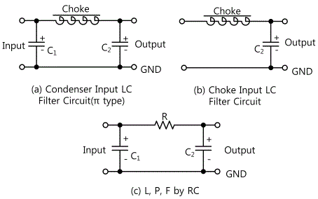
1.Smoothing Circuit Using Choke and Condenser
This method has lower output voltage fluctuation rate by the load than RC Smoothing method and has higher output efficiency. This is because the DC resistance of choke is extremely small so the DC voltage drop by load current is nearly 0 and only the voltage fluctuation rate for the pulsating part exists. However, the AC reactance of choke is big so it can hugely decrease the ripple.
Reference

a. In the smoothing circuit using choke(inductor), the condenser input type can gain the DC voltage which is higher(less than √2 times) than AC voltage of rectifier input. However, choke input type rather outputs slightly lower voltage(less than 1/√2 times).
b. Choke input type has smaller output voltage fluctuation rate than condenser input type, so it is used when voltage stability is needed or in case of DC power supply circuit of over thousands volt which cannot use constant voltage.
c. Smoothing circuit using choke has higher output efficiency than the circuit using the resistance. This is because the choke indicates big reactance to the ripple but only the DC resistance of coil affects DC so pure DC voltage drop by the load current is extremely small.
d. When the values of L and C or of R and C are mutually proper, maximum ripple removal efficiency and output efficiency without waste can be raised.
Reference
In case of full-wave,

Here,


2. Smoothing Circuit Using Resistor and Condenser
RC smoothing circuit is cheap and the attaching location is small. However, when the load current is big, the voltage drop at the series filter resistance of the circuit occurs frequently so the voltage fluctuation rate is big and the output efficiency is low. Therefore, it is used in the small load current circuit of under hundreds mA.
One thing to be noteworthy at RC smoothing circuit is that the rate power of R should be reflected in the design. That is, when the current flowing at series resistor is IR, the rate power is W=R∙IR2 and in the actual usage, it becomes double of this value.
a. In the same voltage circuit, as the load current gets bigger, the condenser capacity rather than smoothing choke or resistance should be increased. This is because the choke or the resistance is applied to the ripple rate only and it is worked as disadvantage to the voltage fluctuation rate according to the load current increase..
b. The resistance smoothing circuit is used for the load of small power consumption for which the power efficiency do not have to be considered. This is because the circuit is minimized.
c. In the smoothing circuit composed of L and C, if the value of L is increased and that of C is increased than proper L and C, the output voltage fluctuation rate increases.
Reference-1
Acceptable Design of L and C Value of Smoothing Circuit which is composed of L and C(C is the minimum value)
Design of L(Inductance) Value

Here, if L is calculated,

• Design of C(Capacitance)
![C(uF)≒[(I_L t)/〖0.5r〗_R ]∙〖10〗^4](../image/part10/formal10.9.gif)
Here, IL = Load Current (A), rR = Ripple Rate(%), Pulsating Cycle t is 60Hz full-wave
current so

Reference-2
Acceptable Design of R and C Value of Smoothing Circuit which is composed of R and C(C is the minimum value)
• Design of Resistor Value

Here, KR=25/100 This means that the voltage drop between both ends of smoothing resistance R is set up as 25% of R input voltage.
• Design of Capacitance Value
![C(uF)≒[(I_L∙t)/〖0.12r〗_R ]∙〖10〗^4](../image/part10/formal10.11.gif)
Here, IL = Load Current (A)
rR = Ripple Rate (%)

Experiment Process
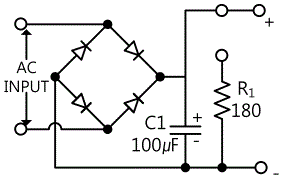
tab1Experiment 10-1.1 Bridge Rectification Circuit Experiment (In Circuit-1 of M10, compose a circuit as in fig. 10-7.)
1.Connection(Circuit-1 of M10)
1.Circuit Connection
Capacitor C1 Connection; Connect between 1g terminal and 1k terminal of Circuit-1 with yellow line.(Wiring diagram. Through 1 step)
2.Power Connection
Connect between Variable Power V1 terminal on the left of M10 board and 1a terminal of Circuit-1 with red line, and between COM terminal and 1b terminal with black line.(Wiring diagram. Through 3 step)
3.Measuring Instrument Connection
Voltmeter Connection
Input Voltage Measurement Connection: - Connect between 1j terminal of Circuit-1 and A+ terminal of Signal Input CH A on the front panel of Multimeter with red line, and between 1n terminal and A- terminal with black line.(Wiring diagram. Through 5 step)
2.Wiring Diagram
3.Measurement
- 1Choose variable power at Touch LCD panel, and click 3 Phase AC Range Power tab.
Click at the right of AC Voltage indication window and make it as 12.0V.
Click and apply the output of 3 Phase AC Range Power to the input of Circuit-1.
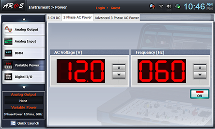
- 2Measure the output wave form and effective voltage with no-load.
Choose analog input on the front panel.
Draw the wave form indicated in Oscilloscope screen in table 10-1.
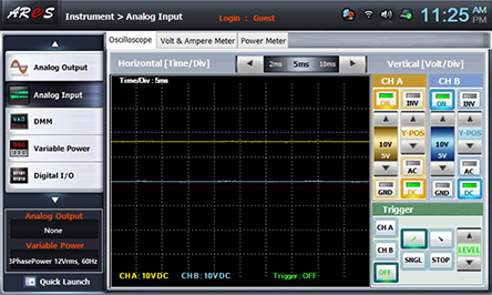
Choose Volt & Ampere Meter tab, click , , at CH A and record the measured output voltage in the relevant column of table 10-1. (CH B is not used.)

- 3Measure the output wave form and effective voltage with load.
Load Connection: Connect between 1i terminal and 1m terminal of Circuit-1 with yellow line.(Wiring diagram. Through 6 step)
Draw the wave form indicated in Oscilloscope screen in table 10-1.

Record the measured value in Volt & Ampere Meter screen in the relevant column of table 10-1.s

After the measurement, click variable power and click to cut off AC 12V
- 4Measure by connecting capacitor C2 additionally.
Capacitor C2 Connection; Connect between 1h terminal and 1l terminal of Circuit-1 with yellow line.(Wiring diagram. Through 6 step)
Execute the measurement process 2), 3) above and record the measured result in the relevant column of table 10-1.(Wiring diagram. Through 7 step)
In case of no-load, remove the connection between 1i terminal and 1m terminal of Circuit-1 and measure
Wiring Diagram
After the measurement, choose variable power and click to cut off AC 12V output.
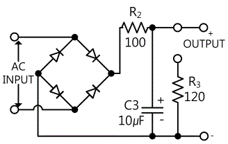
Experiment 10-1.2 Bridge Rectification Circuit Experiment (In Circuit-1 of M10, compose a RC smoothing circuit as in fig. 10-8.)
1.Connection(Circuit-1 of M-10)
1.Circuit Connection
RC Smoothing Circuit Connection; Connect between 1j terminal and 1o terminal of Circuit-1 with red line, and between 1n terminal and 1p terminal with black line.(Wiring diagram. Through 2 step)
2.Power Connection
Connect between Variable Power V1 terminal on the left of M10 board and 1a terminal of Circuit-1 with red line, and between COM terminal and 1b terminal with black line.(Wiring diagram. Through 4 step)
3.Measuring Instrument Connection
Voltmeter Connection
Input Voltage Measurement Connection: Connect between 1q terminal of Circuit-1 and A+ terminal of Signal Input CH A on the front panel of Multimeter with red line, and between 1s terminal and A- terminal with black line.(Wiring diagram. Through 6 step)
2.Wiring Diagram
3.Measurement
- 1Set up as [Capacitor Input Type(C1, C2)]>3. Measurement>1).
- 2Measure the output wave form and effective voltage with no-load
Choose analog input at the front panel.
Draw the wave form indicated in Oscilloscope screen in table 10-2.
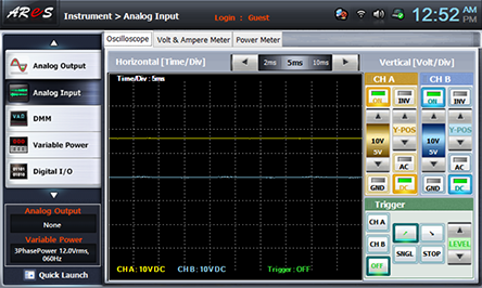
Choose Volt & Ampere Meter tab, click , , at CH A and record the measured output voltage in the relevant column of table 10-2. (CH B is not used.)
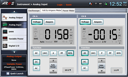
- 3the output wave form and effective voltage with load.
Load Connection: Connect between 1g terminal and 1r terminal of Circuit-1 with yellow line.(Wiring diagram. Through 7 step)
Draw the wave form indicated in Oscilloscope screen in table 10-2.
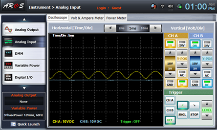
Record the measured value in Volt & Ampere Meter screen in the relevant column of table 10-2.
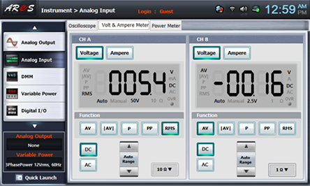
After the measurement, choose variable power and click to cut off AC 12V output.
- 4Capacitor Input RC (π Type) : Measure by connecting capacitor C1 additionally.
Capacitor C1 Connection; Connect between 1g terminal and 1k terminal of Circuit-1 with yellow line.
Wiring Diagram
Execute the measurement process 2), 3) above and record the measured result in the relevant column of table 10-2.
After the measurement, choose variable power and click to cut off AC 12V output.
Experiment 10-1.3
Choke Input Circuit Experiment
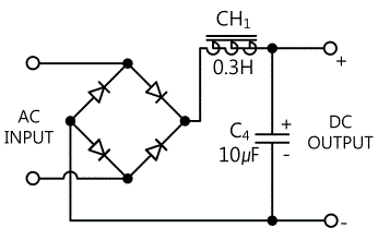
(In Circuit-1 of M10, compose a choke input rectification circuit as in fig. 10-9.)
1.Connection(Circuit-1 of M-10)
1.Circuit Connection
Choke Smoothing Circuit Connection; Connect between 1j terminal and 1t terminal of Circuit-1 with red line, and between 1n terminal and 1u terminal with black line.(Wiring diagram. Through 2 step)
2.Power Connection
Connect between Variable Power V1 terminal on the left of M10 board and 1a terminal of Circuit-1 with red line, and between COM terminal and 1b terminal with black line. (Wiring diagram. Through 4 step)
3.Measuring Instrument Connection
Voltmeter Connection
Input Voltage Measurement Connection: Connect between 1v terminal of Circuit-1 and A+ terminal of Signal Input CH A on the front panel of Multimeter with red line, and between 1x terminal and A- terminal with black line.(Wiring diagram. Through 6 step)
2.Wiring Diagram
3.Measurement
- 1Set up as [Capacitor Input Type(C1, C2)]>3. Measurement>1).
- 2Measure the output wave form and effective voltage with no-load.
Choose analog input at the front panel.
Draw the wave form indicated in Oscilloscope screen in table 10-3.
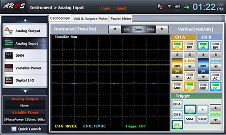
Choose Volt & Ampere Meter tab, click , , at CH A and record the measured output voltage in the relevant column of table 10-3. (CH B is not used.)

- 3Measure the output wave form and effective voltage with load.
Load Connection: Connect between 1v terminal and 1w terminal of Circuit-1 with yellow line.(Wiring diagram. Through 7 step)
Draw the wave form indicated in Oscilloscope screen in table 10-3.
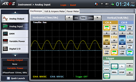
Record the measured value in Volt & Ampere Meter screen in the relevant column of table 10-3.

After the measurement, choose variable power and click to cut off AC 12V output.
Experiment 10-1.4
Capacitor Input LC(π Type) Circuit Experiment
(In Circuit-1 of M10, measure by adding capacitor C1 to the choke input LC circuit as in fig. 10-10.)
1.Connection(Circuit-1 of M-10)
1.Circuit Connection
Capacitor C1 Connection; Connect between 1g terminal and 1k terminal of Circuit-1 with yellow line.
2.Wiring Diagram
Execute the measurement process 2), 3) above and record the measured result in the relevant column of table 10-3.
4.Calculation
1. Maximum Value of Bridge Rectification Output
The maximum voltage of the signal which went through the rectifier is same as the maximum of AC in case of ideal diode and is same as √2 times of AC effective value. In case of approximate analysis, diode voltage drop 1.4V should be subtracted.
Maximum Value of Bridge-rectified Output VP=√2 V
2. DC Output of Bridge Rectification Circuit
DC value of rectified full-wave signal indicated in the secondary part is same as ‘the average value of pulsating current’ or ‘2/π of maximum value’ or 0.9 times of effective value.

3. Output Frequency
The frequency of rectified signal is double of input frequency. This is because one input cycle makes 2 peaks and 2 valleys.

4. Inverse Voltage of Diode
Regardless of the existence of condenser, the maximum value of input is applied to the cutoff diode in case of the diode used in the bridge rectification circuit.
Diode Reverse Voltage:
5. DC Output Voltage of Capacitor Input Smoothing Circuit

Size of Ripple Voltage
6. DC Output Voltage of Choke Input Smoothing Circuit

Ripple Voltage


