PART7Amplifier Circuit(Transistor AMP)
Experiment 4 :Complementary Amp
Theory
Complementary Symmetry(2 Power Supplies)
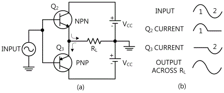
Complementary symmetry circuit uses 2 transistors having same characteristic. However, one is PNP and the other is NPN. Fig. 7-11 shows ideal complementary symmetry push-pull amplifier. Q2 is NPN and Q3 is PNP transistor, and each is the emitter follower where emitter is connected to each other. The load RL of emitter circuit is common to both Q2 and Q3, and the collector of Q2 goes to straight polarity power +VCC and the collector of Q3 gets DC voltage from negative power -VCC.
Q2 and Q3 are supposed to be DC biased to be cut off. During straight polarity change (1), the base of Q2 is operated positively compared to the emitter, and NPN transistor Q2 is turned on. During this straight polarity change (1), Q2 is turned on and the current wave form of Q2 is same as fig.7-11(b). During the positive change, PNP transistor Q3 is reverse biased and cut off, and during the negative change (2), when Q2 is cut off, Q3 is forward biased and turned on. Fig. 7-11(b) shows the direction of current of Q3 is contrary to that of Q2. This is because Q2 is NPN, and Q3 is PNP transistor. The arrow of fig. 7-11 (a) shows the electron and current direction of Q2, Q3 and load RL. The voltage of RL’s both ends is sine wave form just as the input. The operations of Q2 and Q3 are executed separately and they are symmetrical so fig. 7-11 (a) is called complementary symmetry. Complementary symmetry circuit can be composed as emitter-common just as collector-common.
Complementary symmetry amplifier should be designed carefully to prevent thermal runaway or destruction of power transistor. Imbalance or leakage of power transistor can increase errors. Usually, stabilized thermal compensation by diode is used. This condition can be composed by connecting drive terminal and output terminal.
Complementary Symmetry(1 Power Supply)
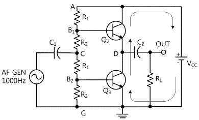
In complementary symmetry push-pull amplifier in fig. 7-12, only one power is used. The symmetry of circuit is maintained by 2 same voltage distributors, R1 and R2. Upper drive terminal provides forward bias to Q2 and lower drive terminal to Q3, and to remove crossover distortion of each transistor, low unemployed current should flow.
The arrow in fig. 7-12 show the path of this unemployed current in the external circuit of Q2 and Q3. The path of unemployed current includes Q3, Q2 and power supply. Q2 and Q3 are supposed to have same characteristics so point D is the middle of the circuit’s DC voltage, that is, VAD=VDG=Vcc/2. In the same way, if the resistances of R1s are same and the resistance of R2 is same and if Q2 and Q3 have same characteristic, point C is the middle of the voltage distributor between point A and G. Therefore, the DC voltmeter connected to point C and D becomes 0V because C and D are on the same DC potential to the earth. According to the voltage distribution of R1 and R2, the value of point B1 is positive compared to point C and D. Therefore, the base(B1) of Q2 is positive compared to the emitter(D) and it provides forward bias so that low unemployed current flows to Q2(NPN).
The ratio of R1 and R2 is an important factor to determine forward bias to flow low unemployed current to Q2 and Q3. The input signal is connected as C1 to the bases of Q2 and Q3 and provides same signal to the base. The capacitor C2 connects output signal to RL and prevents DC current from flowing to RL. Q2 is forward biased according to the straight polarity change of the signal and the flow of current is indicated as straight polarity in both ends of RL. Q3 is forward biased according to the negativity of signal and the negativity is shown in both ends. In fig. 7-12, the operation of other parts is same as the case of using 2 power supplies.
Complementary symmetry push-pull amplifier is used in the output terminal of high output audio amplifier. In this system, speaker voice coil is used as the load and it put in the location of RL. It can be designed for the capacitor C2 to be removed and for the load to be connected between the emitter and the earth. This is possible because the output impedance of emitter follower design is low.
tab1Experiment 7-4.1 Complementary Amp Measurement (Compose in Circuit-2 of M-07.)
1.Connection(Circuit-2 of M-07)
1.Power Connection
It is connected internally.
2.Measuring Instrument Connection
Plug in BNC cable to Signal Output of front panel and connect red line to 2a terminal of AC input of Circuit-3, and black line to 2b terminal.
Measuring input voltage: Connect between 2a terminal of Circuit-2 and A+ terminal of Signal Input CH A on the front panel of Multimeter with red line, and between 2b terminal and A- terminal with black line.
Measuring output voltage: Connect between 2j terminal of Circuit-2 and B+ terminal of Signal Input CH B on the front panel of Multimeter with red line, and between 2k terminal and B- terminal with black line.
2.Wiring Diagram
flash
3.Measurement
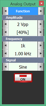
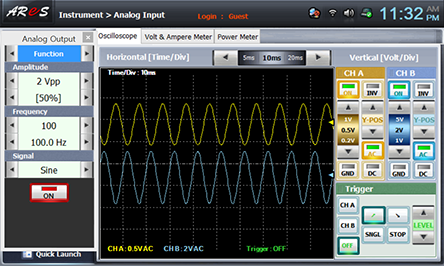
- 1Set up R1 as maximum and choose analog output on the left of front panel, click Function Generator and set up Amplitude Range as , Amplitude as amplitude 40%, Frequency as , Signal as and click to output 1kHz 0.8Vpp.
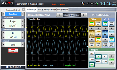
- 2Click analog input at the front panel and set up to indicate input/output wave form in oscilloscope screen.
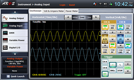
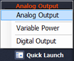
- 3Click quick launch on the left bottom of the screen, choose Analog Output and click at 40% to increase output voltage. Increase it until the signal wave form of CH B is not distorted, draw the wave form of Oscilloscope, calculate distortionless output voltage of CH B and record it in the relevant column of table 7-8.
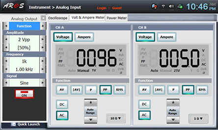
- 4Set up the frequency as 100Hz and measure the output(VPP) of no load and record it in the relevant column of table 7-8.

- 5Connect between 2j terminal and 2l terminal of Circuit-2 with yellow line, measure the output when the load is 50Ω(R6) and record it in table 7-8. If the output is distorted, indicate it in the relevant column of table 7-8.
- 6Wiring Diagram
flash

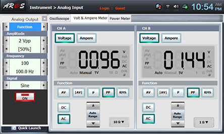
- 7Change the input frequency as 300, 1000, 3000, 10000Hz and repeat process 4), 5) and record the result in table 7-8.
- 8Using the voltage measurement function of separate Digital Multimeter, measure C-E voltage of Q2, Q3 and measure B-E Bias and record it in the relevant column of table 7-8.
Connect red lead wire to 2f terminal of Circuit-2, and black lead wire to 2h terminal and measure C-E voltage of Q1.
Connect red lead wire to 2h terminal of Circuit-2, and black lead wire to 2m terminal and measure C-E voltage of Q2.
Connect red lead wire to 2g terminal of Circuit-2, and black lead wire to 2h terminal and measure B-E Bias voltage of Q1.
Connect red lead wire to 2g terminal of Circuit-2, and black lead wire to 2h terminal and measure B-E Bias voltage of Q1.
Experiment Result Report
1. Experiment Result Table
1) Input / Output wave form in case of 1KHz distortionless maximum output
2. Review and Explanation
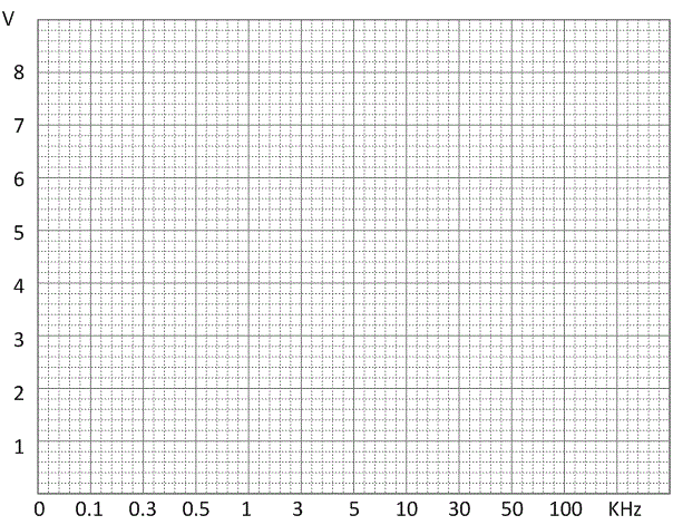
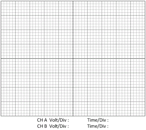
1) Using no load output voltage and load output voltage per frequency in table 7-8, draw frequency characteristic curve in the graph below.