PART6Semiconductor-2
Experiment 2 :MOS FET
Theory
The gate of MOSFET is a capacitor which is very small and excellent, and the conductance through channel is controlled by the voltage applied between the gate and the source. Therefore, compared to that of J-FET, the input current of MOSFET is the leakage current of capacitor which conflicts to the input current, and is also the leakage current of reverse biased p-n junction. Therefore, input impedance of MOSFET is dozens times bigger than that of J-FET.
The gate of MOSFET is made by depositing SiOV2 layer of insulated material on the entire surface of channel, and metal material is put on this thin SiOV2 layer. Fig. 6-6 shows typical structure of MOSFET.
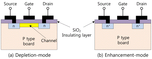
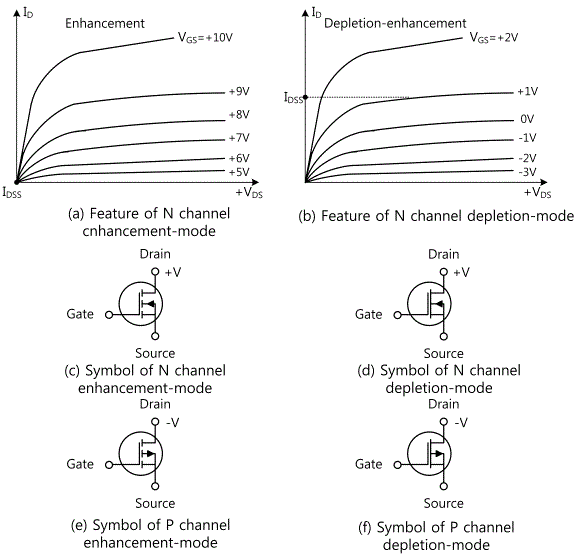
MOSFET can be categorized by detailed structure as depletion-mode and enhancement-mode. Fig. 6-7 (a) shows the characteristic of n channel MOSFET. In depletion mode, the channel is a normal conductor so as in J-FET the current flow can be decreased or cutoff by applying enough gate voltage. In enhancement mode, the channel is normally cutoff but it can be increased or decreased and controlled by applying gate voltage. Depletion mode MOSFET can be operated in enhancement mode as in fig. 6-7 (d).
The capacity of gate is very small so the input impedance is very high. Therefore, the gate can be easily charged over certain voltage level and the narrow SiO2 dielectric of capacitor can be damaged. It is damaged by the voltage of about 50V, and this means that it can be induced by electric charges generated by normal treatment. With these reasons, these elements short the leads and make them as packages.
The inherent capacitance between gate and drain, and between gate and source(deducting high frequency response) is generally lower at MOSFET so the high frequency response is normally better than JFET. While JFET has input leakage current which increases exponentially according to temperature, the effect of temperature is minimum with MOSFET. MOSFET is a semiconductor element which can be commonly used and which is hardly affected by temperature.
Experiment Process
tab1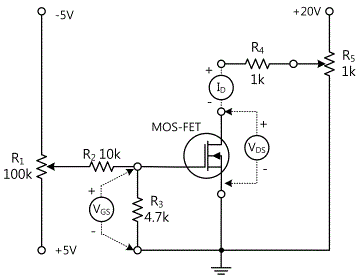
Experiment 6-2.1 MOS FET Characteristic Measurement (In Circuit-2 of M-06, compose a circuit as in fig. 6-8.)
1.Connection(Circuit-2 of M-06)
1.Power Connection
It is connected internally.
2.Measuring Instrument Connection
Ammeter Connection
Measure by using the current measurement function of separate Digital Multimeter.
Measuring the current(ID) flowing on the drain: Connect the red line of Digital Multimeter to 2i terminal of Circuit-2 and the black line to 2g terminal.
Voltmeter Connection
Measuring the voltage(VGS) of R3’s both ends: Connect between 2e terminal of Circuit-2 and A+ terminal of Signal Input CH A on the front panel of Multimeter with red line, and between 2f terminal and A- terminal with black line.
Measuring the voltage (VDS) between drain and source: Connect between 2g terminal of Circuit-2 and B+ terminal of Signal Input CH B on the front panel of Multimeter with red line, and between 2h terminal and B- terminal with black line.
2.Wiring Diagram
flash
3.Measurement
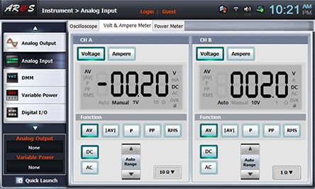
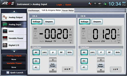
- 1Choose analog input at the left menu of Touch LCD panel, click Volt & Ampere Meter and click , , for CH A and CH B each.
Adjust variable resistance R5 to make VDS as 10V, and adjust variable resistance R1 and change VGS as in table 6-3 and measure ID to record in table 6-3.
When changing VGS by adjusting variable resistance R1, if VDS changes from 10V, adjust variable resistance R5 to make it as 10V and start the measurement.
Next, fix VGS as -0.3V, change VDS as in table 6-4 and measure drain current ID and record the result in table 6-4.

In table 6-4, change VDS for each VGS and measure drain current ID and record it in table 6-4.


4.Calculation
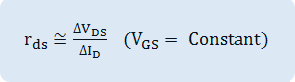
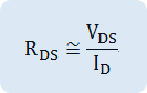
1. Referring table 6-1 and 6-2, calculate dynamic drain resistance, static drain resistance and transconductance.
Experiment Result Report
1. Experiment Result Table
2. Review and Explanation
1) With the measured value of table 6-3 and table 6-4, draw a graph in Graph 6-2.
2) In Graph 6-2 and table 6-3, calculate dynamic drain resistance when VGS= 0V.
3) In table 6-4, calculate static drain resistance when VGS= 0V.
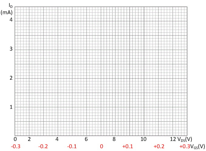 Graph 6-2
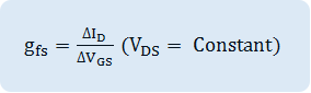
4) Transcoductance gfs can be measured as the change of drain current for change of VGS. In table 6-3, calculate the transconductance for VGS change from –0.1V to –0.2V.