PART6Semiconductor-2
Experiment Purpose
- 1.Investigate characteristics of germanium and silicon diodes.
- 2.Observe the characteristic of zener diode and learn how to use it as voltage stabilizer.
- 3.Investigate the characteristic of SCR through experiment.
- 4.Investigate characteristics of PNP transistor and NPN transistor through experiment.
- 5.Investigate characteristics of J-FET and MOS-FET and through experiment.
Experiment 1 :Junction FET (JFET)
Theory
J-FET is composed of n type or p type channel and gate, which is the opposite material of channel. The physical structure and names of 3 terminals of FET are in fig. 6-2 (a). The drain terminal and source terminal are normally exchangeable and they are determined by how they are connected to the polarities of power voltage. In n channel element, drain is the terminal connected to the positive of the battery, and in p channel element, it is connected to the negative.
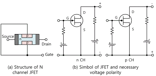
In J-FET and bipolar transistor, there are broad similarities between gate and base, drain and collector, and source and emitter. However, the electrical conduction at J-FET is controlled by reverse bias voltage to gate-source junction, and electrical field is generated as a result.
The conduction control of bipolar transistor is executed by base current at base-emitter junction which is forward biased. This could explain high input impedance of J-FET because the input(gate) of J-FET is a reverse biased junction.
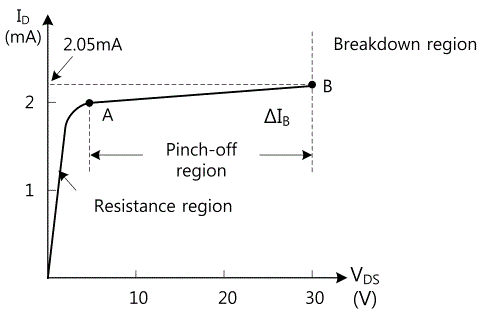
Fig. 6-3 shows the characteristic curve between drain current ID versus voltage VDS between drain and source. In this case, bias voltage, that is, the voltage between gate and source, VGS is “0”.In the first region from“0” to A, that is, in the ohmic region, J-FET operates just as ordinary resistance. The current increase linearly as the applied voltage increases. This operation occurs between 1V and 3V range till pinch-off region begins. Within this range(from A to B), the reverse bias to p-n junction between gate and channel is the cause of depletion region. Till the reverse bias becomes big enough to reach pinch-off region, the depletion region does not widen enough to meet each other. When the bias is applied enough so that two regions meet each other, electric charge is depleted in the channel and pinch-off occurs. Pinch-off means the region where the flow of current is almost constant though VDS changes radically According to fig. 6-3, in the region between A and B, the curve becomes almost horizontal. As the width of channel decreases to 0, the current tends to decrease, and this causes the incline of voltage to be eased following the channel. This reduces the width of depletion region and increases the current. The final value becomes stable value of current and it reaches equilibrium.
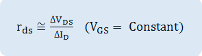
Dynamic Drain Resistance
rds is defined as the curve’s incline in pinch-off region.
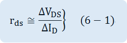
This value is very high and rds between A point and B point of fig. 6-3 is as below.
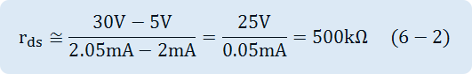
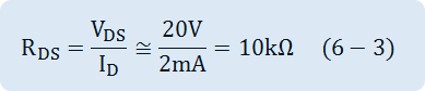
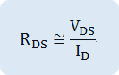
This is VDS, a changing resistance, so it becomes the AC resistance of channel. Meanwhile, under given VDS, the static or DC resistance(RDS) of channel has low resistance value and it can be calculated simply by the ratio of ID to VDS. Therefore, in fig. 6-3, if VDS=20V, it is as below.
The breakdown region of the voltage over B point is also in fig. 6-3. The breakdown occurs when avalanche breakdown occurs to reverse biased gate-channel p-n junction. This is similar to constant voltage region of zener diode, and this is not damaged unless the rated power of FET is exceeded. It is interesting that as the value of VDS increases, J-FET is seen as resistance(resistance region) at first, then as constant current generator(pinch-off region), and finally as constant voltage generator (breakdown region).
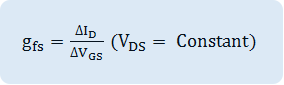
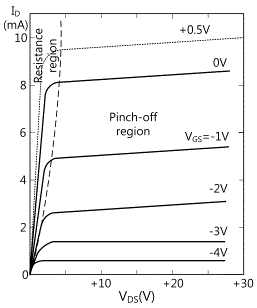
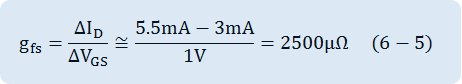
The gate and the source have same electric potential(VGS=0). If the table of ID to VDS are made at different VGS values, as a result, the drain characteristic curve in fig. 6-4 will be made. Bu convention, the breakdown(zener) region is not indicated on the curve and it is because J-FET hardly operates in this region. Note that various bias electric potential(VGS) finally ends as the decrease of drain current value within pinch-off region. This becomes the cause of J-FET’s amplification, and here, the transconductance gfs is measured as the change of drain current to change of VGS.
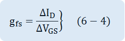
In fig. 6-4, it is indicated that the interval of ID to I-V change by bias voltage is not same. Like this, the transconductance can be changed within certain range. In certain type of FET, every element is in proportion to gs, so this variability can cause problems. The transconductance expressed by the characteristic in fig. 6-4, by VGS change from -1V to -2V, is as below.
Also, note that when gate-channel junction is not in conductive status, the operation by small forward gate-source bias is permitted. FET is usually made of silicon material so this means that positive voltage does not exceed about 0.5V. Of course conduction means important flow of current and this becomes the cause of damage in the element because of warming-up effect in p-n junction.
It does not matter for J-FET whether n channel is used or p channel is used, but usually n channel is adopted. P channel element is operated by the conduction of holes while n channel is operated by the conduction of electron. .Since other factors are same but the mobility of electron is bigger than that of hole, it can be operated within higher frequency. Also, compared to p channel, smaller noise is delivered to the circuit in n channel. Characteristic curve of n channel in fig. 6-4 can be applied same to p channel element. However, all voltage polarity should be in opposite.
Experiment Process
tab1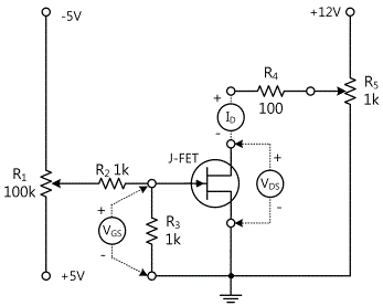
Experiment 6-1.1 JFET Characteristic Measurement (In Circuit-1 of M-06, compose a circuit as in fig. 6-5.)
1.Connection(Circuit-1 of M-06)
1.Power Connection
It is connected internally.
2.Measuring Instrument Connection
Ammeter Connection
Measure by using the current measurement function of separate Digital Multimeter.
Measuring the current(ID) flowing on the drain: Connect the red line of Digital Multimeter to 1i terminal of Circuit-1 and the black line to 1g terminal.
Voltmeter Connection
Measuring the voltage(VGS) of R3’s both ends: Connect between 1e terminal of Circuit-1 and A+ terminal of Signal Input CH A on the front panel of Multimeter with red line, and between 1f terminal and A- terminal with black line.
Measuring the voltage (VDS) between drain and source: Connect between 1g terminal of Circuit-1 and B+ terminal of Signal Input CH B on the front panel of Multimeter with red line, and between 1h terminal and B- terminal with black line.
2.Wiring Diagram
flash
3.Measurement
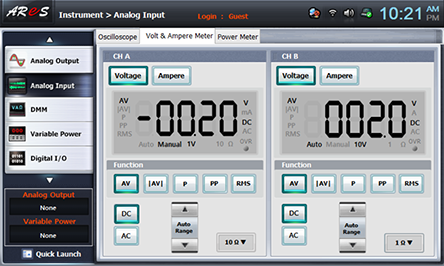
- 1Choose analog inputat the left menu of Touch LCD panel, click Volt & Ampere Meter and click , , for CH A and CH B each.
Adjust variable resistance R5 to make VDS as 10V, and adjust variable resistance R1 and change VGS as in table 6-1 and measure ID to record in table 6-1.
When changing VGS by adjusting variable resistance R1, if VDS changes from 10V, adjust variable resistance R5 to make it as 10V and start the measurement.
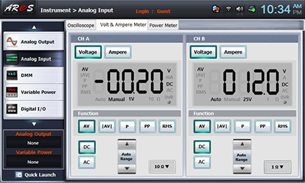
Next, fix VGS as -0.2V, change VDS as in table 6-2 and measure drain current ID and record the result in table 6-2.

In table 6-2, change VDS for each VGS and measure drain current ID and record it in table 6-2.


4.Calculation
1. Referring table 6-1 and 6-2, calculate dynamic drain resistance, static drain resistance and transconductance.
Experiment Result Report
1. Experiment Result Table
2. Review and Explanation
1) With the measured value of table 6-1 and table 6-2, draw a graph in Graph 6-1.
2) In Graph 6-1 and table 6-2, calculate dynamic drain resistance when VGS= 0V.
3) In table 6-1, calculate static drain resistance when VGS= 0V.
4) Explain the difference between dynamic drain resistance and static drain resistance.
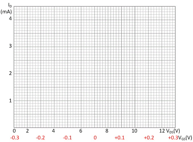 Graph 6-1
5) Transconductance gfs can be measured as the change of drain current for change of VGS. In table 6-1, calculate the transconductance for VGS change from –0.1V to –0.2V.