PART5Semiconductor
Experiment 4 :PNP Transistor
Theory
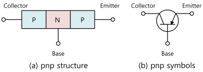
Pnp transistor is composed of two p materials and a n material, as in Fig. 5-11(a). One area of p material is called collector, and another area is called emitter, and the n area in the middle is called base. Fig. 5-11 (b) indicates the signs.
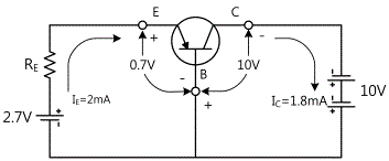
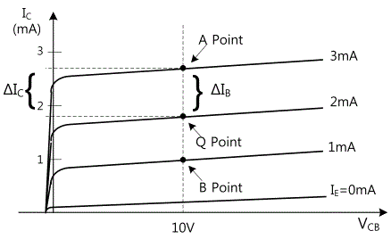
Fig. 5-13 shows the pnp transistor circuit that the base-emitter junction is forward biased, and base-collector junction is reverse biased in CB structure. The resistance is for restricting the current flow in the circuit.
The DC emitter current IE is calculated by subtracting 0.7(in case of silicon VEB from 2.7V and dividing this by RE, and the result is 2V/1KΩ=2mA. The transistor connected as in Fig. 5-12 is called a common base(CB) type, and this is because the base is common to both sides of the circuit. The characteristic curve of CB circuit is expressed in Fig. 5-13.This curve is the expression of relationship between the impressed VCE and the collector current to various values of input emitter current. In this curve, from 2mA of emitter current and 10V of base-collector junction reverse-biased voltage, 1.8mA of collector current is decided.
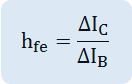
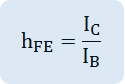
In CB circuit, there is an important relationship between the collector and the emitter currents. The collector current is the output current and the emitter current is the input current so IC/IE is called DC CB forward current gain and its signal is a or hFB. Here, forward current gain is expressed as hFB.
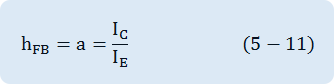
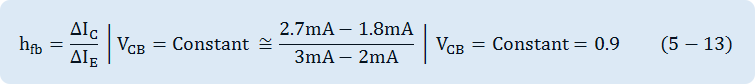
In the circuit of picture 5-12, hFB becomes 1.8mA/2.0mA, that is, 0.9. The representative value of hFB is within 0.9~0.99 and always less than 1.
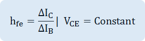
If AC signal is impressed to the input part(emitter) in the circuit of Fig. 5-12, the AC value hfb of CD forward current gain is important(Mind the lower case subscript hfb for the AC). The current gain is defined as below.
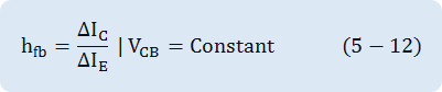
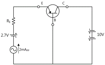
Fig. 5-14 shows CB circuit of Fig. 5-12 with AC input current of 2mAp-p. 2mAp-p current is from the emitter current that changes near certain DC bias level. This bias level(in this case, 2mA) is called quiescent current and for brevity, Q point. Fig. 5-13 expresses this and here, emitter current changes at 3mA and 1mA( A and B points of Fig. 5-13), which is near the quiescent current of 2mA. AC current gain (hfb) can be calculated as below from the curve in Fig. 5-13.
In this case, hfb is calculated between A and Q points of Fig. 5-13, but is same as calculated between B and Q points. Here the DC current gain and AC current gain are same. In actual, both values are not exactly same. In CB circuit, the current gain is slightly smaller than 1, but the voltage gain is quite big.
Experiment Process
tab1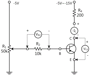
Experiment 5-4.1 PNP Transistor Characteristic Measurement (In Circuit-4 of M-05, compose a circuit as in Fig. 5-15.)
Measuring (IC) Flowing between R4 and Collector
1.Connection(Circuit-4 of M-05, Fig. 5-15)
1.Power Connection
Connect between V1 terminal of Variable Power on M04 board and VCE 5V~15V 4a(+) terminal of Circuit-4 with red line, and between com terminal and 4b(-) terminal with black line.
2.Measuring Instrument Connection
Ammeter Connection
Measure by using the current measurement function of separate Digital Multimeter.
Measuring the current (IC) between R3 and collector: Connect the red line of Digital Multimeter to 4l terminal of Circuit-3 and the black line to 4m terminal.
Voltmeter Connection
Measuring the voltage of resistance R2’s both ends: Connect between 4d terminal of R2 and High terminal of Multimeter on the front panel with red line, and between 4e terminal and Low terminal with black line.
2.Wiring Diagram
flash
3.Measurement
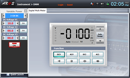
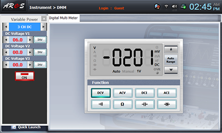
- 1Choose dmm at the left menu of Touch LCD panel and click .
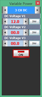
- 2Choose dmm at the bottom of Touch LCD panel and click Variable Power, then 3 CH DC screen appears.
Choose and click at the right of 00.0V to set up the input voltage as DC 10.0V and adjust the voltage value(voltage of R2’s both ends) indicated at Digital Multimeter as Variable Resistance R1 to make it 100mV, then record the current value of separate Digital Multimeter in table 5-7.
Execute the Variable Resistance R1 adjustment and measure by 100mV interval till 800mV.
Variable Resistance R1 is impressed with -5V, so adjust R1 to make IB as - 10μA.
IB is the base current and calculated by the formula below.
-IB=VR2/R2
Therefore, if IB=10μA, VR2=R2×-IB=10×103×10×10-6=-100mV.
Therefore, if the voltage of R2’s both ends is -100mV, IB is -10μA. When IB=-20μA, estimate by -200mV, and if IB=-80μA, estimate by -800mV for IC.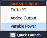
- 3After the measurement, click to cut off the output.
Measuring (IC) Flowing between R3 and Collector
1.Connection(Circuit-4 of M-05, Fig. 5-14)
1.Power Connection is same as [Measuring (IC) Flowing between R2 and Collector]>Connection.
2.Measuring Instrument Connection
Ammeter Connection
Measure by using the current measurement function of separate Digital Multimeter.
Measuring the current (IC) between R3 and collector: Connect the red line of Digital Multimeter to 4j terminal of Circuit-4 and the black line to 4k terminal.
Voltmeter Connection
<Voltmeter Connection> is same as [Measuring (IC) Flowing between R2 and Collector]>Connection.
2.Wiring Diagram
flash
3.Measurement
- 1It is same as [Measuring (IC) Flowing between R4 and Collector]> Measurement and record the measured value in the relevant column of table 5-7.
- 2After the measurement, click to cut off the output.
4.Calculation
1. Draw a graph in Graph 5-5 using values of table 5-6, check out the collector current (IC) flowing to R3, R4 when IB is -40μA and calculate the current amplification factor.(when VCE=10V)
Experiment 5-4.2 PNP Transistor Characteristic Measurement (In Circuit-4 of M-05, compose a circuit as in Fig. 5-14.)
Changing the Base Current IB as 40, 60, 80μA and Measuring the Collector Current between R4 and Collector for each VCE
1.Connection(Circuit-4 of M-05, Fig. 5-14)
1.Power Connection
Connect between V1 terminal of Variable Power on M04 board and VCE 5V~15V 4a(+) terminal of Circuit-e with red line, and between com terminal and 4b(-) terminal with black line.
2.Measuring Instrument Connection
Ammeter Connection
Measure by using the current measurement function of separate Digital Multimeter.
Measuring the current (IC) between R4 and collector: Connect the red line of Digital Multimeter to 4l terminal of Circuit-4 and the black line to 4m terminal.
Voltmeter Connection
Measuring the voltage of resistance R2’s both ends: Connect between 4d terminal of R2 and High terminal of Multimeter on the front panel with red line, and between 4e terminal and Low terminal with black line.
2.Wiring Diagram
flash
3.Measurement
- 1Choose dmm at the left menu of Touch LCD panel and click . Choose dmm at the bottom of Touch LCD panel and click Variable Power, then 3 CH DC screen appears.
Choose and click at the right of 00.0V to set up the input voltage as DC 6.0V and adjust the voltage value(voltage of R2’s both ends) indicated at Digital Multimeter as Variable Resistance R1 to make it -200mV, then record the current value of separate Digital Multimeter in table 5-8.
Click Variable Power and click at the right of 3 CH DC to adjust it to VCE voltage of table 5-8 and record the measured value of current (IC) of separate Digital Multimeter in table 5-8.
If the voltage of R4’s both ends is out of 200mV(400mV, 600mV, 800mV), execute Variable Resistance R1 Adjustment, make it fit to the setup voltage, measure the current (IC) flowing between R4 and Collector and record it.
- 2After the measurement, click to cut off the output.
Changing the Base Current IB as 40, 60, 80μA and Measuring the Collector Current between R3 and Collector for each VCE
1.Connection(Circuit-3 of M-05, Fig. 5-9)
1.Power Connection is same as [Changing the Base Current IB as 40, 60, 80μA and Measuring the Collector Current between R4 and Collector for each VCE]
2.Measuring Instrument Connection
Ammeter Connection
by using the current measurement function of separate Digital Multimeter.
Measuring the current (IC) between R3 and collector: Connect the red line of Digital Multimeter to 4j terminal of Circuit-3 and the black line to 4k terminal.
Voltmeter Connection
<Voltmeter Connection> is same as [Changing the Base Current IB as 40, 60, 80μA and Measuring the Collector Current between R4 and Collector for each VCE].
2.Wiring Diagram
flash
3.Measurement
- 1Execute same as [Changing the Base Current IB as 40, 60, 80μA and Measuring the Collector Current between R4 and Collector for each VCE]>Measurement>1) process and record it in table 5-8.
- 2After the measurement, click to cut off the output.
4.Calculation
1. Draw a graph in Graph 5-6 using values of table 5-8, draw a straight line between -10V of the voltage between collector-emitter (VCE) and -6mA of the collector current (IC), make the point where the base current (IB) is -40uA as Q point and calculate the current amplification factor (hFE) which is the DC current gain for Q point condition.
2. dDraw a vertical line to Q point and make the point where the base current (∆I〗B) is -20uA as A point to calculate 〖∆IB,〖∆IC and calculate AC current gain.
Experiment Result Report
1. Experiment Result Table
2. Review and Explanation
1) Draw a graph in Graph 5-5 using values of table 5-7, check out the collector current (IC) flowing to R4, R3 when IB is -40μA and calculate the current amplification factor.(when VCE=10V)
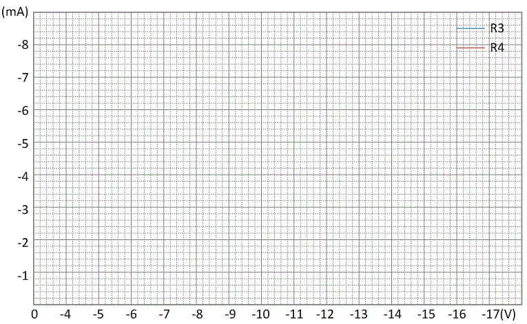
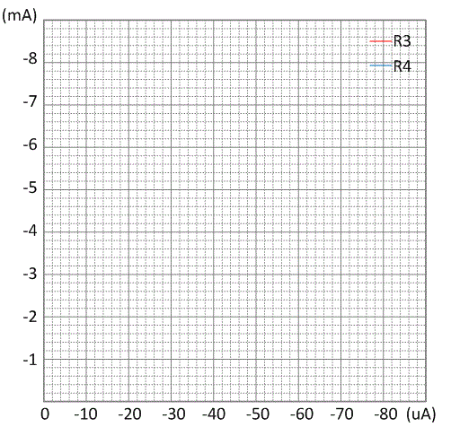 Graph 5-5
2) Draw a graph in Graph 5-6 using values of table 5-8, draw a straight line between 10V of the voltage between collector- emitter (VCE) and -6mA of the collector current (IC), make the point where the base current (IB) is -40uA as Q point and calculate the current amplification factor (hFE) which is the DC current gain for Q point condition.
 Graph 5-6
3) Draw a vertical line to Q point and make the point where the base current (IB) is -20uA as A point to calculate ∆IB,∆IC and calculate AC current gain.