


PART5Semiconductor
Experiment 2 :Characteristic of Zener Diode
Theory
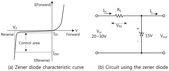
Zener diode is similar to other diodes except it uses reverse yield point. Therefore, the reverse yield point is controlled carefully during the production process and the zener voltage can be any value from 2~3V to over 200V. Fig. 5-5 (a) shows the characteristic curve of zener diode to certain current and voltage. IZK is the minimum reverse current when the diode operates within the breakdown region and IZM is the maximum reverse current which the diode can endure without exceeding rated power. The incline between IZK and IZM is known as zener impedance ZZ. The incline can be calculated by dividing change amount of horizontal axis with that of vertical axis. The changes of voltage, current or other variables can be expressed as Greek character Δ(delta). Therefore, the incline in Fig. 5-5 can be expressed as ΔV/ΔI.
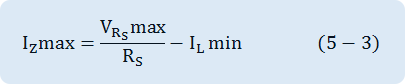
When operating zener diode between IZK and IZM, the voltage of diode’s both ends becomes comparably regular. This principle is used in the circuit of Fig. 5-5(b). 20~30V of unstabilized DC voltage is impressed to the circuit and reverse bias is applied to the zener diode, and it is assumed that if it is over IZK, enough reverse current is supplied so that the diode can be within the coordination area in Fig. 5-5(a). Then, even though the input voltage changes from 20V to 30V, the output voltage will be maintained relatively constant. Therefore, zener diode controls the output voltage and it is put in parallel to the output circuit so it is called a parallel regulator. Note that Vout=Vz In Fig. 5-5 (b), Rs should be chosen properly to maintain zener regulator and to make enough current flow so that needed load current can be supplied. If reverse zener current is operated at IZK, the load changes within certain range. If the load changes from 0 to 100mA and IZK is 100mA at zener diode, when the voltage of R_s both ends is minimum, the current flowing through R_s will be minimum. Therefore, R_s should be small enough to operate the circuit under all conditions and to supply IZK of zener diode and maximum load current of 100mA. Therefore, Rs is decided as below.
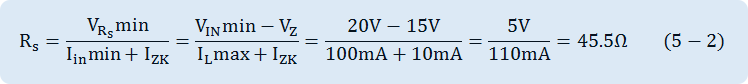
When the minimum value of unstable input (VRs min) is 20V, and the maximum current of 100mA flows at the load, if Rs bigger than 45.5Ω is used, the zener cannot have enough reverse current. Therefore, considering safety factors, it is proper to set up Rs smaller than the calculated value.
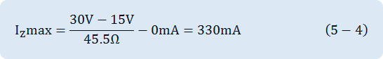
Once proper value is set up to zener diode parallel regulator, it should be made safe so that Rs does not exceed the rated power of zener diode when the current bigger than minimum input voltage or maximum load current flows (The current of zener diode increases when the load current decreases). If the input voltage increases from the minimum value of 20V, the zener voltage is maintained relatively constant so the voltage of Rs both ends increases. Similarly, if the load changes so that the current smaller than 100mA flows, the decreases of load current appears through zener diode. Therefore, at the zener diode of parallel regulator, the maximum power dissipation occurs when the input voltage is maximum and the load current is minimum within the change range. Therefore, in the circuit of Fig. 5-4(b), the maximum zener current for Rs of 45.5Ω is calculated as below.
Here, IL min : minimum load current
LZ maz : maximum zener current
VRs max is from 30V to 15V, and IL min is 0.
Maximum power dissipated at the zener diode is same as the multiplication of zener voltage and zener current.
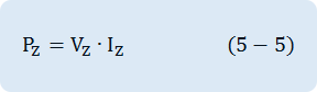
The maximum power dissipated at the zener diode occurs when IZ is maximum. Therefore, PZ=15V×330mA=4.95W.
Experiment Process
tab1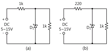
Experiment 5-2.1
6.1V Zener Diode Characteristic Measurement
(In Circuit-2 of M-05, compose a circuit as in Fig. 5-6(a), (b).)
When D1=Zener Diode 6.1V, R1= 1kΩ
1.Connection(Circuit-2 of M-05, Fig. 5-6(a))
1.Circuit Connection
Connect between 2c terminal and 2i terminal of Circuit-2 with yellow line, and between 2e terminal and 2k terminal with yellow line.
2.Power Connection
Connect between V1 terminal of Variable Power on M04 board and 2a(+) terminal of Sig Input & DC Input of Circuit-2 with red line, and between com terminal and 2b(-) terminal with black line.
3.Measuring Instrument Connection
Voltmeter Connection
Voltage Measurement between resistance R3, R4, R5, R6: Connect between 2k terminal of R3 and High terminal of Multimeter on the front panel with red line, and between 2q terminal and Low terminal with black line.
2.Wiring Diagram
flash
3.Measurement
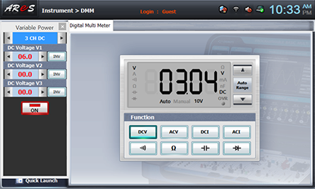
- 1Choose dmm at the left menu of Touch LCD panel and choose .
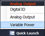
- 2Choose quick launch at the bottom of Touch LCD panel and click Variable Power then 3 CH DC screen appears.
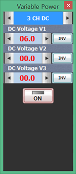
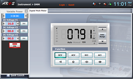
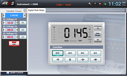
- 3Click at the right of 00.0V in DC Voltage V1 indication window to set up the input voltage as 6V and click and record the voltage value of R3’s both ends indicated at DMM in the relevant column of table 5-3.
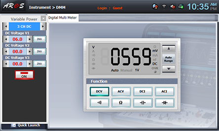
For the voltage of R4’s both ends, move the connection line of 2l to 2l and record the voltage value indicated at DMM in the relevant column of table 5-3.
For the voltage of R5’s both ends, move the connection line of 2m to 2m and record the voltage value indicated at DMM in the relevant column of table 5-3.
For the voltage of R6’s both ends, move the connection line of 2n to 2n and record the voltage value indicated at DMM in the relevant column of table 5-3.
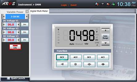
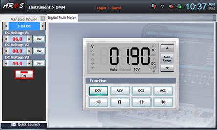
- 4Click at the right of 06.0V inDC Voltage V1 indication window to set up the input voltage as 8V, 10V, 12V, 14V, 16V and execute Measurement 3) process and record the measured value in the relevant column of table 5-3.
- 5After the measurement, click to cut off the output.
When D1=Zener Diode 6.1V, R1= 220Ω
1.Connection(Circuit-2 of M-05, Fig. 5-6(b))
1.Circuit Connection
Connect between 2f terminal and 2i terminal of Circuit-2 with yellow line, and between 2h terminal and 2k terminal with yellow line.
2.Power connection is same as [When D1, R1= 1kΩ]>Connection>Power Connection.
3.Measuring instrument connection is same as [When D1, R1= 1kΩ]>Connection>Measuring Instrument Connection.
2.Wiring Diagram
flash
3.Measurement
- 1Execute same as [When D1, R1= 1kΩ]>Measurement and record in the relevant column of table 5-3.
- 2After the measurement, click to cut off the output.
4.Calculation
1. In the circuit of Fig. 5-6(a) (b), calculate the load current (IL) flowing on the load R3 and the zener current(IZ) flowing on the zener diode.
Experiment 5-2.2
Zener Diode Characteristic Measurement
(In Circuit-2 of M-05, compose a circuit as in Fig. 5-6(a), (b).)
When D2=Zener Diode 9.1V, R1= 1kΩ
1.Connection(Circuit-2 of M-05, Fig. 5-6(a))
1.Circuit Connection
Connect between 2c terminal and 2j terminal of Circuit-2 with yellow line, and between 2e terminal and 2k terminal with yellow line.
2.Power Connection
Connect between V3 terminal of Variable Power on M04 board and 2a(+) terminal of Sig Input & DC Input of Circuit-2 with red line, and between com terminal and 2b(-) terminal with black line.
3.Measuring Instrument Connection
Voltmeter Connection
Voltage Measurement between resistance R3: Connect between 2k terminal of R3 and High terminal of Multimeter on the front panel with red line, and between 2q terminal and Low terminal with black line.
2.Wiring Diagram
flash
3.Measurement
- 1Execute same as [When D1, R1= 1kΩ]>Measurement 1)~4) process and record in the relevant column of table 5-4
- 2After the measurement, click to cut off the output.
When D2=Zener Diode 9.1V, R1= 220Ω
1.Connection(Circuit-2 of M-05, Fig. 5-5(b))
1.Circuit Connection
Connect between 2f terminal and 2j terminal of Circuit-2 with yellow line, and between 2h terminal and 2k terminal with yellow line
2.Power connection is same as [When D1, R1= 1kΩ]>Connection>Power Connection.
3.Measuring instrument connection is same as [When D1, R1= 1kΩ]>Connection>Measuring Instrument Connection
2.Wiring Diagram
flash
3.Measurement
- 1Execute same as [When D1, R1= 1kΩ]>Measurement 1)~4) process and record in the relevant column of table 5-4
- 2After the measurement, click to cut off the output.


4.Calculation
1. In the circuit of Fig. 5-5(a) (b), calculate the load current (IL) flowing on the load R3 and the zener current(IZ) flowing on the zener diode.
Experiment Result Report
1. Experiment Result Table
2. Review and Explanation
1) In the circuit of Fig. 5-5(a) (b), calculate the load current (IL) flowing on the load and the zener current(IZ) flowing on the zener diode with the formula below and record it in the table.
- 1st step: Calculate series current. Is=(V-VZ)/RS
- 2nd step: Judge load voltage. VL=VZ
- 3rd step: Calculate load current. IL=VL/RLc
- 4th step: Calculate zener current. IZ=IS-IL
Rs: Series Resistance
VL: Load Voltage
VZ: Zener Voltage
IZ: Zener Current
Is: Series Resistance Current
IL: Load Resistance Current
2) After the experiment, draw the characteristic curve on Graph 5-1 and 5-2
Red Full Line : VS to VL Voltage Characteristic when R1=RS 1kΩ, R3=RL 1kΩ
Blue Full Line : VS to VL Voltage Characteristic when R1=RS 220Ω, R3=RL 1kΩ
Red Dotted Line : VS to VL Voltage Characteristic when R1=RS 1kΩ, R3=RL 1kΩ
Blue Dotted Line : VS to VL Voltage Characteristic when R1=RS 220Ω, R3=RL 1kΩ
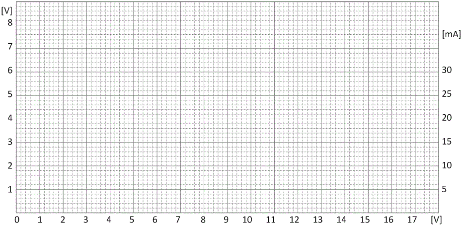
Graph 5-1 (Zener Diode 6.1V Circuit, Characteristic Curve of VS to VL and VS to IL)
Graph 5-2 (Zener Diode 9.1V Circuit, Characteristic Curve of VS to VL and VS to IL)