


PART16Signal Converter
Experiment 4 :V-F Converter
Theory
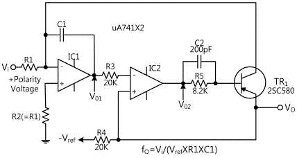
Voltage-Frequency converter(V-F converter) is composed of integration circuit. Fig.16-12 is the circuit of V-F converter, which amplifies the input voltage Vi inversely by IC1 and executes the integration by C1. This integrator executes the feedbackof the reversed current to the input so the output voltage VO can be expressed as below.
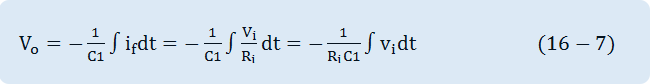
(Here, if is the feedback current.)
The transient response of this circuit is as below when expressed using Laplace Transform.
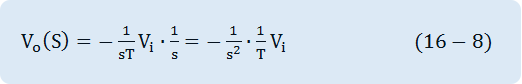
(Here, T is R1C1, and s is the differential operator(=d/dt) Therefore, if V0(t)=L-1[V0(s)] is applied, it is as below.
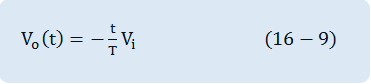
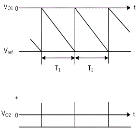
This formula means that the output voltage of the time when t=0 is V0=0, and that of the time after t=T becomes V0=Vi. Here, R2 is the resistance to correct the bias resistance, and it becomes R2 ≅ R1. Therefore, if the time constant of R1C1 is determined, the output waveform is expressed as integrated saw tooth wave as V01 of fig.16-14. Also, IC2 compares the output voltage of integrator and standard voltage Vref and when V01 is lower than Vref, the output voltage of comparator becomes (+) and the transistor TR1 is turned on, and the charge of C1 is discharged to TR1. On the contrary, when VO1 becomes V and passes through the comparing area of IC2, the output voltage is saturation voltage of VO2 (-) and TR1 is turned off.
The integration starts in the direction that VO1 as the time constant of R1C1 becomes 0V. In this case, IC1 is the time constant of R1C1, and when normal integrator is operated TR1 has very small saturation voltage Vr so + voltage of IC2 becomes 0V potential which is same as the voltage of IC1.
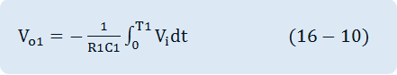
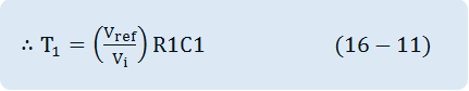
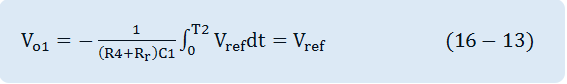
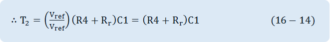
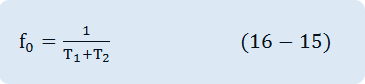
Therefore, in the potential where VO1 is over 0V, IC2 is reversed and TR1 is turned off. The problems of this circuit are that the leakage current of collector should always be integrated when TR1 is turned off, that the leakage current should be small, and that the welding resistance(Rr) of TR1 should be smaller than R1. To determine the output frequency of this circuit, if the period of time at the moment of integration is T1 and the time needed for reset is T2, then T1, T2 and the oscillation frequency are as below.
(Here, R1 is the resistance when TR1 is welding.)
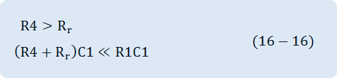
However, actual T2 must have very small time constant comparing to T1.
Therefore, the circuit constant should satisfy the two conditions below.
In the end, the output oscillation frequency to the input voltage of this circuit is influenced greatly by the time constant R1C1, so to setup the standard or oscillation frequency, R1 or C1 should be determined or the standard voltage Vref should be adjusted. However, if Vref is set up to high, the intersecting point with the maximum value of integrated output voltage does not exist and the output does not occur so the voltage should be set up as about half of the integrated output.
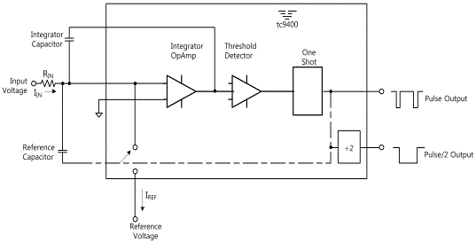
IC for V-F converter circuit is TC9400 and fig.16-15 shows its block diagram.
Experiment Process
1. For the experiment, use Circuit-4 of M-16.
2. Connect between 4a-4b terminals and adjust R4 so that the output frequency becomes 0Hz.
3. Measure the output frequency when voltage value of of input signal is increased by 1V to 4a-4b as in table 16-4 and record the result in the relevant column and test the linearity of input voltage and output frequency.
tab1Experiment 16-4.1 V/F Converter Converter Circuit (Compose as Circuit-4 of M16.)
1.Connection
1.Circuit Connection
In Circuit-4 of M16, connect between 4d-4g, between 4f-4g terminals with yellow lines.
2.Power connection is internally connected.
3.Measuring Instrument Connection
Connect BNC cable to Signal Output on the front panel, connect red lead wire to 4a of Circuit-4 and black lead wire to 4b terminal.
Voltmeter Connection(Zero ADJ Measurement)
On the Multimeter of front panel, connect between High terminal and 4h terminal of Circuit-4 with red line, and between Low terminal and 4j terminal with black line.
Voltmeter Connection(F-OUT)
Connect between 4i terminal of Circuit-4 and A+ terminal of Signal Output on the front panel with red line, and between 4j terminal and A- terminal with black line.
2.Wiring Diagram
flash
3.Measurement
- 1Adjust ZERO ADJ.
Choose dmm at Touch LCD, click and connect between 4a-4b terminals of Circuit-4 with yellow line and adjust R5 so that the output voltage becomes 0V.
- 2Measure the output frequency when voltage value of of input signal is increased by 1V to 4a-4b as in table 16-4 and record the result in the relevant column and test the linearity of input voltage and output frequency.
Connect BNC terminal to Signal Output of front panel, and connect red lead wire to 4a terminal and black lead wire to 4b terminal.
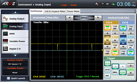
Choose analog output at Touch LCD and choose Oscilloscope tab.
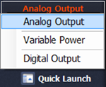
Click quick launch at the bottom left, choose Analog Output and click of function to make DC Source window appear.
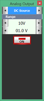
Click at 1v of Range to adjust as the input voltage of table 16-4 and output the frequency by the output waveform and record the result in the relevant column.
4.Calculation
1. Calculate the output frequency following the formula below and record the result in the relevant column of table 16-4.
In Circuit-4, RIN=R1, CREF=C1, VREF=-5V.
FOUT=VIN / RIN ×1 / ((CREF )∙(VREF))
Experiment Result Report
1. Experiment Result Table
Table 16-4
| Input Voltage [㎐] | 1V | 2V | 3V | 4V | 5V | 6V | 7V | 8V | |
|---|---|---|---|---|---|---|---|---|---|
| Output Frequency [mV] | Measurement | ||||||||
| Calculation | |||||||||