


PART15Combination Logic Circuit
Experiment 4 :Adder/ Subtracter
Theory
Half Adder
Half adder is composed of two binary inputs and two binary outputs. The input variables indicate augend and addend, and the output variables indicate sum and carry. Generally, two inputs are called x and y, and two outputs S and C. The truth table for input and output is as table 15-9.

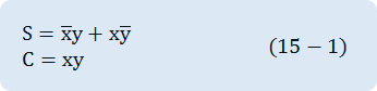
C becomes 1 when both inputs are 1. S becomes 1 when either of the inputs is 1. Simple Boole functions for two outputs can be earned easily from the truth table. The simplified sum of the multiplication is as below.
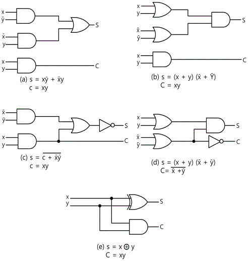
The logical expression of this is fig.15-11 and 4 other logical expressions of half adder are in fig.15-11. These all output same result concerning the operation of input and output. Based on this, we can see that there are various choices even when making a simple combination logic function like this.
Fig.15-11(a) is the implementation of half adder in the sum of multiplication, and (b) is that in the multiplication of sum.
(c) is earned from the truth that S is Exclusive-OR of x and y. The complement of S is the equivalence of x and y.
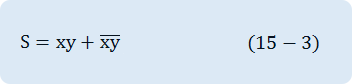
Meanwhile, C=xy, so,
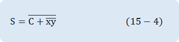
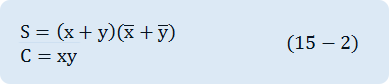
In (d), if C is expressed as the multiplication of sum, it is as below.
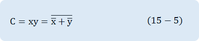
The half adder can be realized as Exclusive-OR gate and AND gate as in (e).
Full Adder
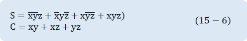
Full adder is a combination circuit that calculates the sum of three input bits. It is composed of three inputs and two outputs. The input variables expressed as x and y are two bits of current position that will be added, and the third input variable expressed as Z is the carry from the previous position. When three bits are added, the sum can become from 0 to 3, and since 2 digits are required to express 2 and 3 as binary numbers so two outputs are needed. Among two outputs, the sum is expressed as S and the carry as C. By calculating the sum of three bits, the previous digits becomes the output carry C and the next digit is expressed as S. The truth table of full adder is as fig.15-12.
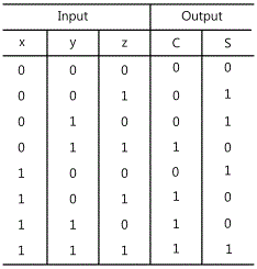
To all the possible combination of 1 and 0 which three input variables can have, two output variables have the value of 1 or 0. When all inputs are 0, the output becomes 0. The output S becomes 1 when 1 or 3 inputs are 1.
The input/output bits of the combination circuit can be interpreted differently at various levels of the problem. The binary signal of the input line is added arithmetically, and it is considered the bit that outputs the sum of two digits to the output line.
On the other hand, in case of expressing as truth table or composing a circuit as a logical gate, the same binary value in the previous sentence can be considered the variable of Boole function. It is important to recognize that the bits used in this circuit can be interpreted differently like this.
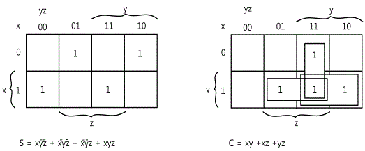
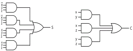
In the input/output logical relationship of full adder circuit, one Boole function corresponds to each output variable so it can be expressed as two Boole functions. To simplify each Boole function, a map is needed for each case. Each map is composed of 8 quadrangles since the output is the function of three input variables. The two maps in fig.15-13 are used to simplify two output functions. The 1 in the quadrangle of each map can be earned directly from the truth table. In case of the output S, the quadrangles expressed as 1 cannot be combined to the adjacent quadrangles so they cannot be simplified. The output C is simplified and earned the expression of 6 characters. The logic diagram of full adder in the sum of multiplication is in fig.15-14. This is made by using the Boole function expression below.
Other compositions for full adder can be developed. If it is expressed as the multiplication of sum, the same number of gates as in fig.15-14 are used, but the number of AND gate and that of OR gate is switched.

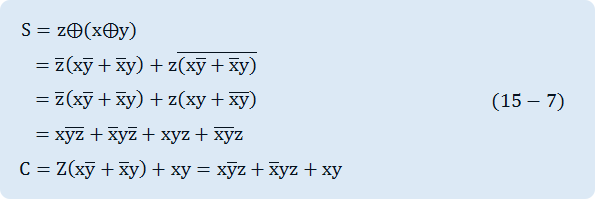
The full adder can be implemented with two half adders and one OR gate as in fig.15-15. The output S of the second half adder is the Exclusive-OR of the output of the first half adder and z. S and C can be expressed as Boole function as below.
Half Subtracter
Half subtracter is a combination circuit that subtracts between two bits and calculates the difference. This circuit has another output that shows whether 1 is borrowed or not. x is used to express the subtracted bit, and y the subtracting bit. To calculate x-y, the relative sizes of x and y should be considered. If x≥y, three cases below are possible. Those are 0-0=0, 1-0=1, and 1-1=0. This result is called the difference bit. If x<y, That is, 0-1, 1 should be borrowed from the previous digit. The borrowed 1 is same as 2 in binary number so is added to the bit of subtracting number and eventually, 2-1=1. The half subtracter needs two outputs, one for generating the difference and expressing as the sign D, and the other for expressing the borrowing with the sign B and indicating the borrowing of 1 from previous digit. The truth table for half subtracter is as fig.15-16.
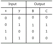
The output B is 0 when x≥y, and becomes 1 only when x=0, y=1. The output D is the result of the arithmetic operation 2B+x-y. The Boole functions for two outputs of half subtracter can be calculated directly from the truth table.
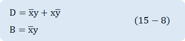
The logic for D is same as that for S in half adder.
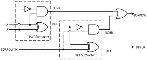
Full Subtracter
Full subtracter is a combination circuit that executes subtracting between two bits considering the borrowed 1 for the previous low level. This circuit has three inputs and two outputs. x, y, z are used to indicate subtracted number, subtracting number and borrow from previous digit. The truth table of full subtracter is as fig.15-17.
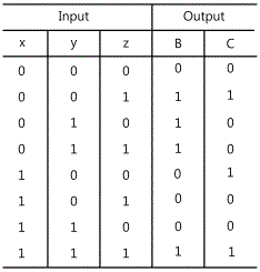
To all possible combinations of 1 and 0 that three input variables can have, the values of two output variables are determined as “1” or “0” according to the result of x-y-z. When the input borrow(z) is 0, it becomes same as half subtracter. If x=0, y=0, z=1, 1 should be borrowed from the previous digit. In that case, 2 is applied to x so it becomes 2-0-1=1 and D=1, and because there is a borrow, B becomes 1, too. When x=0, yz=11, 1 should be borrowed from the previous digit so B=1, and 2 is added to x so D becomes 0 by 2-1-1=0. When x=1, yz=01, x-y-z=0 so B=0, D=0. Finally, if x=1, yz=11, 1 is borrowed from the previous digit and 2 is added to x and it becomes 3 so D=1, B=1.
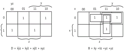
The Boole functions for two outputs of full subtracter is in the map of fig.15-18. If this is simplified and expressed as the sum of multiplication, it is as below.
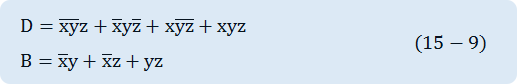
It is interesting that the output S of full adder is same as the output D of full subtracter, and the output B of full subtracter can be same if x is substituted by x. Therefore, if the complement of x is applied to the gate that calculates the carry, the full adder can be changed to the full subtracter easily.
Experiment Process
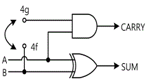
1. In Circuit-4 of M-15, connect between 4f-4g terminals and compose a half adder as in fig.15-19.
2. When the input A, B are same as table 15-6, record the output Sum(4l) and Carry(4h) in the relevant column.
tab1Experiment 15-4.1 Adder/Subtracter Circuit Experiment (Circuit-4 of M15)
Half Adder Circuit: In Circuit-4 of M-15, compose a half adder as in fig.15-19.
1.Connection
1.Circuit Connection
Half Adder Input: In Circuit-4 of M15, connect between Q0 terminal of Digital Output on front panel and 4a terminal, between Q2 terminal and 4b terminal with red lines, and between COM terminal and GND terminal with black line.
In Circuit-4, connect between 4f-4g terminals with yellow line.
2.Power connection is internally connected.
2.Wiring Diagram
flash
3.Measurement
- 1When the input A, B are same as table 15-7, record the sum of output(Sum(4n))and the carry(Carry(4h)) in the relevant columns.
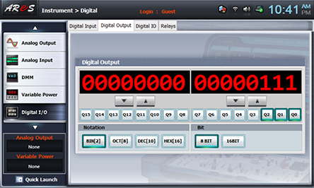
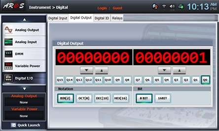
Choose digital i/o at Touch LCD panel, click Digital Output tab, choose at Bit, and click Q0, Q1 corresponding to the input data of table 15-7 so record the result of red LED(carry) and green LED(sum).(Q0 output corresponds to A input of half adder and Q1 output to B input.)

4.Calculation
1. Make a logical expression for output sum and carry.
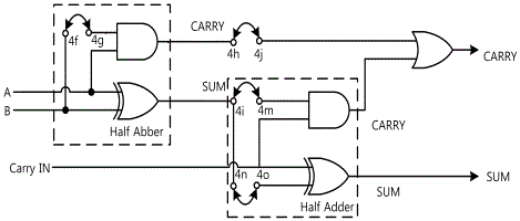
Full Adder Circuit: In Circuit-4 of M-15, compose a full adder as in fig.15-19.
1.Connection
1.Circuit Connection
Full Adder Input: In Circuit-4 of M15, connect between Q0 terminal of Digital Output on front panel and 4a terminal, between Q2 terminal and 4b terminal with red lines, and between COM terminal and GND terminal with black line.
Full Adder Carry Input: Connect between Q2 terminla of front panel Digital Output and 4c terminal with red line.
In Circuit-4, connect between 4f-4g, 4h-4i, 4l-4m, 4n-4o terminals with yellow line.
2.Power connection is internally connected.
2.Wiring Diagram
flash
3.Measurement
- 1When the input A, B, Carry are same as table 15-8, record the sum of output(Sum(44))and the carry(Carry(4p)) in the relevant columns.
Choose digital i/o at Touch LCD panel, click Digital Output tab, choose at Bit, and click Q0, Q1,Q2 corresponding to the input data of table 15-8 so record the result of red LED(carry) and green LED(sum).(Q0 output corresponds to A input of full adder, Q1 output to B input, and Q2 to carry input.)
4.Calculation
1. Make a logical expression for output sum and carry.
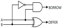
Half Subtracter Circuit: In Circuit-4 of M-15, compose a half subtracter as in fig.15-21.
1.Connection
1.Circuit Connection
Half Subtracter Input: In Circuit-4 of M15, connect between Q0 terminal of Digital Output on front panel and 4a terminal, between Q2 terminal and 4b terminal with red lines, and between COM terminal and GND terminal with black line.
In Circuit-4, connect between 4d-4f, 4e-4g terminals with yellow line.
2.Power connection is internally connected.
2.Wiring Diagram
flash
3.Measurement
- 1When the input A, B are same as table 15-9, record the difference of output(Differ(4n))and the borrow(Borrow(4h)) in the relevant columns.
Choose digital i/o at Touch LCD panel, click Digital Output tab, choose at Bit, and click Q0, Q1 corresponding to the input data of table 15-9 so record the result of red LED(borrow) and green LED(difference).(Q0 output corresponds to A input of half subtracter and Q1 output to B input.)
4.Calculation
1. Make a logical expression for output difference and borrow.
Full Subtracter Circuit: In Circuit-4 of M-15, compose a full subtracter as in fig.15-22.
1.Connection
1.Circuit Connection
Full Subtracter Input: In Circuit-4 of M15, connect between Q1 terminal of Digital Output on front panel and 4a terminal, between Q2 terminal and 4b terminal with red lines, and between COM terminal and GND terminal with black line.
Full Subtracter Borrow Input: Connect between Q0 terminal of Digital Output on front panel and 4c terminal with red line.
In Circuit-4, connect between 4d-4f, 4e-4g, 4h-4i, 4l-4j, 4m-4k, 4n-4o terminals with yellow line.
2.Power connection is internally connected.
2.Wiring Diagram
flash
3.Measurement
- 1When the input A, B, Borrow are same as table 15-10, record the output difference(Diffier(4r)) and the borrow(Borrow(4p)) in the relevant columns.
Choose digital i/o at Touch LCD panel, click Digital Output tab, choose at Bit, and click Q0, Q1, Q2 corresponding to the input data of table 15-10 so record the result of red LED(borrow) and green LED(difference).(Q0 output corresponds to borrow input, Q1 output to A input of full subtracter and Q2 to B input of full subtracter.)

4.Calculation
1. Make a logical expression for output difference and borrow.