PART8Basic Electrical Circuit
Experiment 2 :Complimentary Symmetrical Amplifier
Theory
The amplifier can be categorized as small-signal amplifier and large-signal amplifier.
The small-signal amplifier amplifies the signal whose amplitude changes little(from several to several hundreds mV) with the operating point as center. This sets up the operating point near the center of linear operating area of the transistor and uses it so the linearity of input-output signal is important.
The large-signal amplifier is called power amplifier that amplifies the signal whose amplitude is big. The output of the amplifier can be distorted by nonlinear characteristic of the transistor so the bias method different form that of small-signal amplifier is necessary in order for the linearity to be maintained in big dynamic range. Also, power conversion efficiency, rated power, safe working area, heat caused by power consumption are important
The amplifier can be categorized as class A, class B, class AB, and class C.
Class A Bias Amplifier
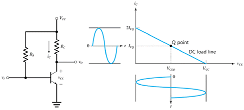
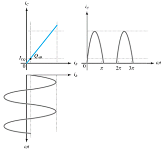
- As in fig.8-9, the operating point is set up near the center of linear area of collector current, and the whole period of input current is amplified without distortion and outputted as collector current, which means the linearity of this is good.
- Regardless of the input current, the bias current ICQ always flows so the DC power consumption(VCEQICQ) by this is big ad the power efficiency is low.
Class B Push-Pull Amplifier
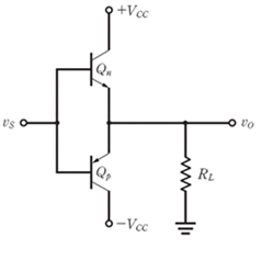
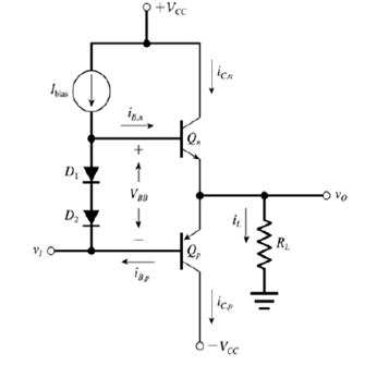
- This is used to heighten the efficiency of power conversion and manage the signal of big amplitude, and as in fig.8-10, this is composed as a complementary structure of NPN type BJT(n channel MOSFET) and PNP type BJT(p channel MOSFET). Each transistor has a class B bias whose operating point is set up at the cutoff point and two BJTs are assumed to have ideal characteristics
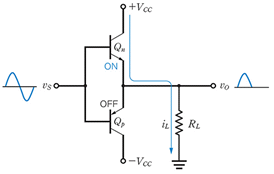
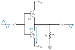
- As in fig.8-11, the signal of whole period can be earned using the complementary push-pull circuit and since the bias current ICQ is 0, DC power consumption is theoretically 0 so the power efficiency of this is higher than that of class A amplifier.
Crossover Distortion
The actual BJT has the voltage drop of VBE(on)≈0.7V of emitter-base junction, and the transistor Qn and Qp are all cut off at -0.7a≤Vs≤0.7 and the output becomes 0 so the distortion occurs at the output waveform as in fig.8-12. This distortion is called cross over distortion.
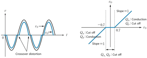
(a) Input and output voltage (b) Delivery characteristic curve of in/output
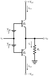
(a) Class AB bias of push-pull amplifier
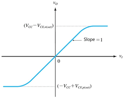
(b) Delivery characteristic curve of in/output
To remove the crossover distortion of class B push-pull amplifier, class AB bias is used as in fig.8-13.
Class AB Bias Amplifier
As in fig.8-14, this is the amplifier whose operating point is moved toward class A bias. This is used to remove the distortion of output waveform by VBE voltage drop of class B push-pull amplifier, and the power efficiency of this is smaller than that of class B amplifier and bigger than that of class A amplifier.
Class AB Bias Push-Pull Amplifier Using Diode
In the circuit as in fig.8-15, the bias voltage VBB of Qn and Qp is generated by the voltage drop occurred at diode D1 and D2.
Class C Bias Amplifier
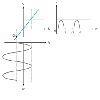
As in fig.8-16, this is the circuit that the operating point is set up below the cutoff point of the transistor, parts of half period of the input signal come out as the output, and the rest half period is cut off so its distortion of the output waveform is the most severe.
The sine wave with distortion includes the components of harmonics so if LC tuning circuit is used at the output of amplifier, the components of fundamental wave without the harmonics can be earned. It has the smallest average value of collector current so the power efficiency is the biggest.
Experiment Process
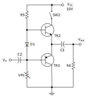
1. Make a connection as in fig.8-17.
2. Connect the function generator to the input terminal Vin, and apply the frequency 1kHz, 10Vpp voltage.
3. Connect the terminal of D1’s both ends with yellow line. (Short of D1)
4. Connect + part of DC voltage to the emitter part of TR2 using the separate digital multimeter, connect GND to – part and adjust VR1 to make the voltage as 5V.
5. Draw the waveform of the output voltage in the relevant column of table 8-2 when the input voltage is increased in the range that the output waveform is not distorted and record the output voltage.
6. Remove the left cable of the diode and measure the voltage applied to the diode using DC voltmeter.
- Record the output waveform and voltage in table 8-2.
7. Adjust VR1 to make the output voltage as 3V.
- Adjust the input voltage and draw the waveform outputted at the oscilloscope.
- Is the half wave where the distortion first occurs a + waveform or a – waveform?
8. Adjust VR1 to make the output voltage as 7V.
- Adjust the input voltage and draw the waveform outputted at the oscilloscope.
- Is the half wave where the distortion first occurs a + waveform or a – waveform?
tab1Experiment 8-2.1 Push-Pull Amplifier Experiment (In Block b of M07, compose a circuit as in fig.8-17.)
1.Connection(Block b of M08)
1.Circuit Connection
In Block b of M08, connect between the upper terminal and lower terminal of D1 with yellow line.
Connect between the right terminal of C3 and upper terminal of R6 with yellow line.
2.Power Connection
Connect between V1 termiinal of Variable Power on the left of M08 board and V+ terminal of Block b with red line, and between COM terminal and the earthing terminal with black line.
3.Measuring Instrument Connection
Function Generator Connection
Connect between A+ terminal of Signal Output on front panel and the left terminal of C2 of Block b on M08 with red line, and between A- terminal and the earthing terminal of Block b with black line.
Voltmeter Connection
Input Measurement: Connect between A+ terminal of Signal Input CH A on front panel and the left terminal of C2 of Block b with red line, and between A- terminal and the earthing line with black line.
Output Measurement: Connect between B+ terminal of Signal Input CH B on front panel and the right terminal of C3 of Block b with red line, and between B- terminal and the earthing line with black line.
Emitter Voltage(VA) Measurement: At DC voltage measurement of the searate digital meter, connect the red (+) lead wire to the right terminal of TR2 of Block b, and the black (-) lead wire to the earthing terminal.
2.Wiring Diagram
3.Measurement
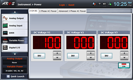
- 1Choose variable power at left menu of Touch LCD panel and set up at 3 CH DC for DC Voltage V1 to become 10V.
Click , and supply the output of DC 10V to the circuit.
Turn on the SW2.
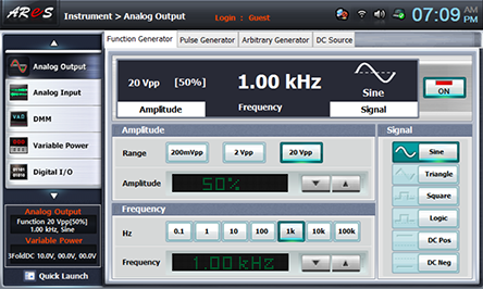
- 2Choose analog output at left menu of front panel, click Function Generator and set up Amplitude as , amplitude 50% , Frequency as , Signal as and click to output 1kHz 10Vp-p.
- 3Connect + part of DC voltage to the emitter part of TR2 using the separate digital multimeter, connect GND to – part and adjust VR1 to make the voltage as 5V.
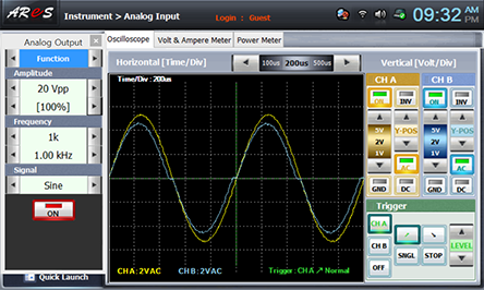
- 4Choose analog input at left menu of Touch LCD panel, choose Oscilloscope tab and choose , , for CH A and CH B each.
Increase the input voltage in the range that the output waveform of the amplifier is not distorted.
Draw the output waveform(CH B) in the relevant column of table 8-2 and record the output voltage.

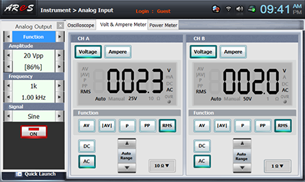
- 5Remove the left cable of the diode(D1) and measure the voltage applied to the diode using the voltmeter of the separate digital multimeter and record the result in the relevant column of table 8-2.
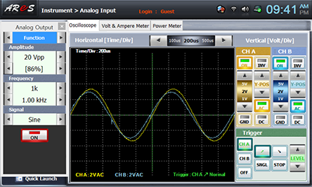
Choose analog input at left menu of Touch LCD panel, choose Oscilloscope tab and draw the output waveform(CH B) in the relevant column of table 8-2 and record the output voltage.
- 6Connect + part of DC voltage to the emitter part of TR2 using the separate digital multimeter, connect GND to – part and adjust VR1 to make the voltage as 3V.
Execute the measurement process 4) above.
- 7Connect + part of DC voltage to the emitter part of TR2 using the separate digital multimeter, connect GND to – part and adjust VR1 to make the voltage as 7V.
Execute the measurement process 4) above.


- 8After the measurement, choose variable power at left menu of Touch LCD panel, click to cut off the power supply, and click at analog output to cut off the function generator.
Experiment Result Report
1. Experiment Result Table
Voltage between D1’s both ends : (V)


