PART8Basic Electrical Circuit
Experiment Purpose
- 1.Understands amplifier and multistage amplifier.
- 2.Understands characteristic of cascade amplifier.
- 3.Understand constant voltage circuit, relay and touch control switch.
Experiment 1 :Amplifier
Theory
Amplification
As in fig.8-2, when small electrical signal is applied to the input terminal, big electrical signal appears at the output terminal, and this is called the amplification and the device to execute this is called the amplifier.
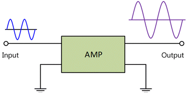
This means that the signal itself does not gets bigger but the output of amplifier gets proportionally bigger to the input signal.
When the signal is applied to the input terminal of the amplifier, the purpose of amplifier is to amplify the signal as we desire. For example, if AC signal is applied, the output that is the same type as the input signal should be amplified at the output terminal, but in the actual situation, it is not. There are several reasons for this.
Experiment Process

As in fig.8-3, if AC signal is applied to the amplifier, the output that is the same type as the input signal should be amplified at the output terminal. However, at the output terminal, the waveform that is distorted as dotted line is amplified, and this is called distortion.
- The amplitude distortion is caused by incorrect bias operating point, excessive input signal, no straight characteristic curve, incorrect load value and so on, so the input signal should be applied to the operating point of A level or the bias or the load value should be chosen correctly.
- The frequency distortion is caused at the output by lots of harmonics occurred at the active element, and this phenomenon means the change of amplitude due to the circuit constant by the frequency. If possible, the active element which contains less harmonics should be used and the circuit constant proper to the frequency should be selected.
- The phase distortion is caused by the combination between the preference reaching to the input directly and that reaching later due to various causes. This is a big problem in the high frequency area but does not matter in the low frequency area, that is, in the sound equipment.
- The signal appears at the output side though it is not applied to the input, and this is called noise and there are various kinds of noises such as the noise caused by the element, mechanical noise, electrical noise and so on. There are various measured for noise removal, such as using circuit element that has correct value, or doing the complete shielding by reducing the capacity between parts. In case of parasitic oscillation, neutralizing circuit should be used.
Amplification Circuit of Transistor
There are C-B(common base) circuit, C-E(common emitter) circuit, and C-C(common collector) circuit.
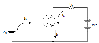
- C-B(Common Base) Circuit
Common base circuit is the circuit that the base is commonly connected to both the input and output of the circuit. The base should be earthed and the input signal should be applied between the emitter and the base so the output is earned between the base and the collector.
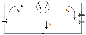
In fig.8-4, the direction of the arrow is that of the current and IE=IC+IB(A) is valid. Here, the power(bias) should be applied so that the current can flow in the arrow direction. Supply by comparing the direction of IE and the polarity of VEE and the direction of IC and the polarity of VCC.
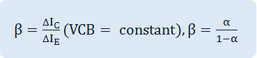
The amplification factor α of this amplifier is
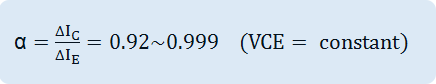
This amplifier has the lowest input impedance and highest output impedance, and its current amplification degree is nearly 1 and the voltage amplification degree is big. Also, its cutoff frequency is high so it is used frequently in the high frequency amplification circuit.
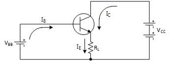
- C-E(Common Emitter) Circuit
This is the circuit that the emitter is earthed and the input voltage is applied to the base and the output is earned at the collector. To understand C-E circuit, the characteristic of the circuit between the input terminals or between the base emitters, or the circuit between the output terminals or between the collector emitters.
In fig.8-5, the direction of the arrow is that of the current and even though the composition of the transistor changes, the relationship between the currents are not different from that of C-B circuit.
That is, IE `=IC` `+IB(A) and IC = alpha IE(A)
The amplification factor β of this amplifier is
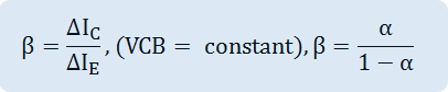
Ifαis indicated by β, it is α= β/(1+β)..
The characteristic of this amplifier is that its amplification degrees of current and voltage are over 1, and its input and output impedances are the middle of collector earthing and base earthing. The input and output impedance do not change much according to the signal source and load resistance, and the amplification factors of current and voltage are efficiently big so this is generally used in the amplification circuit.
- C-C(Common Collector) Circuit
Common collector circuit is usually called emitter follower, and it has load(output) resistance between the emitter and the earthing. The shape is similar to C-E circuit but the difference is that the collector is earthed. The direction of arrow in fig.8-6 indicates the direction of the current, and C-C circuit, contrary to C-B or C-E circuits, has big input impedance and small output impedance so is used in the impedance matching circuit, and its output characteristic is same as that of C-E circuit.
The characteristic of this circuit is that its input impedance is big and output impedance is small so it is proper to be combined with the circuit having low input impedance(impedance matching). Also, the voltage phase of input and output is same and the gain is below 1, the current phase of input and output is reversed and the gain is big. This is 100% negative feedback amplifier that is stable and whose distortion is the smallest.
Transistor Bias Circuit
Bias means the device that can be operated as an amplifier by applying DC voltage to the transistor amplifier and flowing DC current. The amplification of transistor is possible when proper DC voltage is supplied and DC current flows.
- Types of Bias
There are base bias, emitter bias, negative feedback bias and the combination bias of these kinds.
Generally, emitter bias or negative feedback bias are widely used, which solve the problem of base bias that the bias changes according to the temperature of surroundings or of the transistor itself.
Voltage Division Bias Circuit
Fig.8-7 is called voltage distribution bias circuit or current feedback bias circuit, which divides the power voltage of the circuit Vcc with R1 and R2 resistances and gets the bias voltage VBE by the voltage drop of R4 resistance connected to the emitter.
When the input signal is applied to the base, the change of base current occurs by changes of emitter current and collector current.
AV=VO/Vi , the current gain is Ai = IO / Ii, and the power gain is AP = AO / Ai = PO / Pi.

Experiment Process

1. Make a connection as the circuit in fig.8-8.
2. Turn on the switch of the circuit and measure the voltage VBE, VCE, VEE of TR1 and record the result in the relevant column of table 8-1.
3. Measure the voltage between R3’s both ends and calculate the collector current IC using the measured voltage and Ohm’s law.
4. Connect the function generator to the input terminal Vin and measure with the oscillator the output voltage of the collector when applying the voltage of 1kHz, 0.5Vpp and record the result in the relevant column of table 8-1. Calculate the voltage gain and record the result.
5. Measure the emitter output voltage with the oscilloscope and record the result in the relevant column of table 8-1. Calculate the voltage gain and record the result.
6. Draw the input voltage(Vin) waveform and output voltage(VCE, VEE) waveform in the relevant column of table 8-1 when the input voltage(>0.5Vpp) is increased in the range that the output waveform(VCE) is not distorted and record the output voltage.
- Calculate the voltage amplification degree with measured input voltage and output voltages of collector and emitter.
tab1Experiment 8-1.1 Amplifier Experiment (In Block a of M07, compose a circuit as in fig.8-8.)
1.Connection(Block a of M08)
1.Power Connection
Connect between V1 terminal of Variable Power on the left of M08 board and V+ terminal of Block a with red line, and between COM terminal and the earthing terminal with black line.
2.Measuring Instrument Connection
Function Generator Connection
Connect between A+ terminal of Signal Output on front panel and the left terminal of C1 of Block a on M08 board with red line, and between A- terminal and the earthing terminal of Block a with black line.
Voltmeter Connection
Collector Voltage(VCE) Measurement: Connect between A+ terminal of Signal Output CH A on front panel and the lower terminal of R3 of Block a with red line, and between A- terminal and the earthing terminal of Block a with black line.
Emitter Voltage(VEE) Measurement: Connect between B+ terminal of Signal Output on front panel and the lower terminal of R4 of Block a with red line, and between B- terminal and the earthing terminal of Block a with black line.
Base Voltage(VBE) Measurement: Connect between High terminal of Multimeter on front panel and the upper terminal of R2 of Block a with red line, and between Low terminal and the earthing terminal with black line.
2.Wiring Diagram
flash
3.Measurement
- 1Choose variable power at left menu of Touch LCD panel and set up at 3 CH DC for DC Voltage V1 to become 10V.
Click , and supply the output of DC 10V to the circuit.
Turn on the SW1.
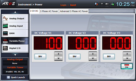
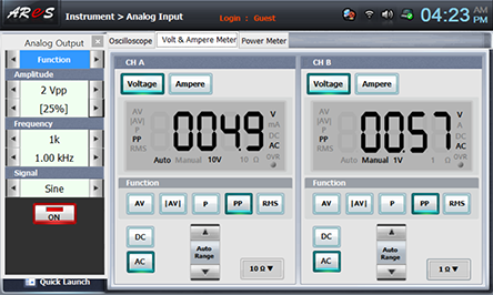
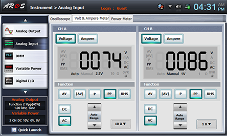
- 2Choose analog input at left menu of Touch LCD panel and click Volt & Ampere Meter tab. Click , , for CH A and CH B each.
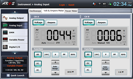
Record the measured values in CH A and CH B in the relevant columns of table 8-1. Here, CH A is the collector voltage(VCE) and CH B the emitter voltage(VEE).
- 3Choose dmm at left menu of Touch LCD panel and click .
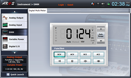
This is the base voltage(VBE), so record it in the relevant column of table 8-1.
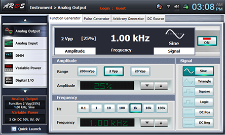
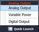
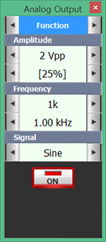
- 4Choose analog output at left menu of front panel, click Function Generator and set up Amplitude as , amplitude 25% , Frequency as , Signal as and click to output 1kHz 0.5Vp-p.
- 5In the connection for emitter voltage(VEE) measurement, change the connection between B+ terminal of Signal Input CH B on front panel and the upper terminal of R4 of Block a as between B+ terminal and the left terminal of C1 of Block a. Leave the connection of the earthing terminal.
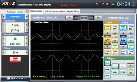
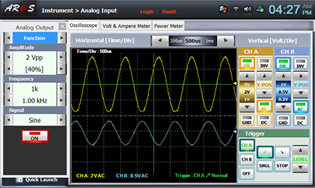
- 6Click analog input at front panel, click Oscilloscope tab so that the input/output waveform appears on the screen.
The waveform of CH A is (VCE) output waveform and the waveform of CH B is that of input waveform. Record them at Input/Output Waveform 1 in table 8-1.
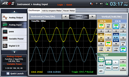
The waveform of CH A is (VCE) output waveform and the waveform of CH B is that of input waveform. Record them at Input/Output Waveform 1 in table 8-1.
Choose Volt & Ampere Meter tab, click , for CH A and CH B each, and record the measured input/output voltage value at Input/Output Waveform 1 in table 8-1.
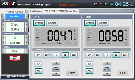
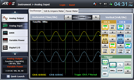
- 7Change the connection of red line from A+ terminal of Signal Input CH A on front panel to lower terminal of R3 of block a for the collector voltage(VCE) measurement from A+ terminal to upper terminal of R4 and click Oscilloscope tab to observe the waveform.
The waveform of CH A is (VEE) output waveform, and that of CH B is the input waveform. Record them at Input/Output Waveform 2 in table 8-1.
Click Volt & Ampere Meter tab and record the measured input/output voltage value at Input/Output Waveform 2 in table 8-1.
- 8Connect the cable again as below.
Collector Voltage(VCE) Measurement: Connect between A+ terminal of Signal Output CH A on front panel and the lower terminal of R3 of Block a with red line, and between A- terminal and the earthing terminal of Block a with black line.
Input Voltage Measurement: Connect between B+ terminal of Signal Output on front panel and the left terminal of C1 of Block a with red line, and between B- terminal and the earthing terminal of Block a with black line.
- 9Click quick launch at left bottom menu of Touch LCD panel, choose Analog Output and click 25% of to increase the output voltage. Increase it till the signal waveform of CH B is not distorted, draw the waveform of Oscilloscope, calculate the input voltage of CH A and distortionless output voltage of CH B and record it at Input/Output Waveform 3 in table 8-1.

Change the connection of red line from A+ terminal of Signal Input CH A on front panel to lower terminal of R3 of block a for the collector voltage(VCE) measurement from A+ terminal to upper terminal of R4, and measure the oscilloscope waveform and voltage to record at Input/Output Waveform 4.
- 10After the measurement, choose variable power at left menu of Touch LCD panel, click to cut off the power supply, and click at analog output to cut of the function generator.
Experiment Result Report
1. Experiment Result Table
Voltage of R3’s both ends = (V+)-(VCE), Collector current(Ic)=(voltage of R3’s both ends)/R3
2. Review and Explanation
1) Calculate the amplification rate β using Input/Output Waveform 1 and 3 in table 8-1 above.