PART7Basic Circuit of Semiconductor
Experiment 6 :Characteristic of Transistor
Theory
Bipolar transistor is the transistor that two pn junctions are attached so that n or p area can be shared, and there are pnp type and npn type according to the type of attachment. Fig.7-22(a) shows schematic explantion of pnp type transistor. The operation principles of two types are similar so here, pnp type will be explained. The most basic function of transistor is amplification and to amplify, proper bias voltage should be applied to the transistor. For the amplification, forward voltage is applied to one between two pn junctions and reverse voltage is applied to the other. At pnp type transistor, the p area of the junction to which forward voltage is applied is called emitter, and that to which reversed voltage is applied is called collector, and the n area in the middle is called base. Fig.7-22(b) shows the circuit symbol of pnp type transistor, and in case of npn type, the direction of the arrow should be reversed.
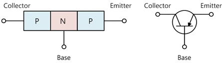
(a) Structure of pnp (b) Symbol of pnp
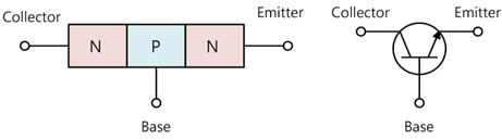
(a) Structure of npn (b) Symbol of npn
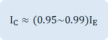
When forward voltage is applied between the emitter and the base, then as in the diode, the positive hole is injected from p type to n type and the electron fron n type to p type. In pnp type transistor, the positive hole injected from p type to n type plays a main role. In normal diode, the positive hole injected to n area is connected again to the electrons that are plenty in n area and consumed. However, the base area of transistor is very thin so most of the positive holes reach to collector junction before it is reconnected. In collector junction where reverse voltage is applied, strong magnetic field is applied and this magnetic field makes the positive holes injected to the collector junction move to collector area. In the end, in pnp type transistor, the positive holes emitted from the emitter are mostly collected at the collector.
This can be explained as below by the size of current. In fig.7-24, the emitter curret IE is generated by the positive holes and electrons injected by the forward voltage applied at the emitter junction, and in case of pnp type, the transistor is designed so as the current by the positive hole can be much bigger. And most of these positive holes pass through the collector junction, so in the end the collector current IC has similar size as IE. Actually, it becomes as below.
(1)
By Kirchhoff’s law of node,
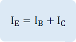
(2)
So, the base current IB = IE - IC is small compared to IE or IC, and this is generated by the small ratio of positive holes reconnected in base area among the electrons injected from the base to the emitter and the positive holes injected from emitter to base. Therefore, the ratio of collector current and base current
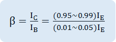
(3)
has pretty big value, and this is the reason that the transistor can execute the current amplification.
Earthing of Transistor
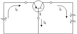
When the transistor is used in the amplification circuit, two input electrodes and two output electrodes are needed, but the transistor has only three electrodes so one of them should be shared. According to which electrode is shared, there are base earthing(common-base or grounded-base), emitter earthing and collector earthing. Fig.7-24 shows base earthing and fig.7-25 emitter earthing.
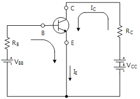
Emitter earthing can amplify both the current and the voltage so it is used most commonly. Emitter earthing can amplify both the current and the voltage so it is used most commonly.
Characteristic Curve of Emitter Earthing
There are input characteristic curve and output characteristic cuve for current-voltage characteristic of the transistor, and usually the characteristic curve means the output characteristic curve. In case of emitter earthing, the input characteristic curve means the relationship between the input current IB and the input voltage VBE, and this is usually similar to the characteristic curve of the diode and becomes slightly different according to the output voltage VCE.
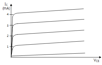
The output characteristic curve means the relationship between the output current IC and output voltage VCE, and at small VCE, IC increases according to the increase of VCE. However, if VCE exceeds certain level, the increase speed becomes very slow, and this is called saturation region. At small VCE, the amount of positive holes gathered to the collector according to the increase of VCE increases. However, once most of the positive holes transferred from the emitter are gathered at the collector, the amoung of positive holes gathered to the collector is not increased even though VCE increases.
Under same VCE , the value of IC is depenant upon the number of positive holes transferred from the emitter area so it changes according to the value of VBE or IB. Therefore, as in fig.7-26, various characteristic curves can be drawn according to the value of IB.
Experiment Process

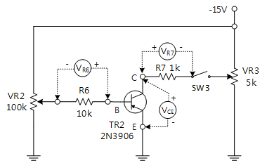
1. Using Block c of M07 board, make a connection as in fig.7-27.
- TR1 is NPN type and TR2 is PNP type.
2. Set up the input power as +15V. VR2 adjust the base current of TR1 and VR3 supplies the voltage between the collector and the emitter.
3. Locate VR3 in the middle, turn VR2 slowly to the right and measure with DC voltmeter so that the voltage applied to R6 becomes 0.1V.
4. Here, the base current is calculated as I= VR6 / R6 = 0.1V / 10k Ω = Ω =10uA.
5. Connect DC voltmeter between C and E of TR1 and turn VR3 slowly and adjust so that 1V can be measured.
6. Record the voltage measured at R7 in the relevant column of table 7-10.
7. Calculate the collector current flowing through R7 using Ohm’s law and record the result in the relevant column of table 7-10.
I C = VR7 / R7
8. To make the base current as 20uA, turn VR2 to the right and set up as 0.2V.
9. Execute 5~7 processes above to measure and record.
10. To make the base current as 20uA, turn VR2 to the right and set up as 0.2V.
11. Execute 5~7 processes above to measure and record.
tab1Experiment 7-6.1 Experiment of NPN Emitter Earthing Characteristic
1.Connection(Block c of M07)
1.Circuit Connection
Connect between V+ terminal of Block c and the terminal connected to VR2 with red line.
Connect between lower terminal of R6 of Block c and the base terminal of TR1 with yellow line.
Connect between the collector terminal of TR1 of Block c and upper terminal of R7 with yellow line.
Connect between the emitter terminal of TR1 of Block c and earthing terminal with yellow line.
2.Power Connection
Connect between +15V terminal of Fixed Power on the left of M07 board and V+ terminal of Block c with red line.
Connect between GND terminal of Fixed Power on the left of M07 board and earthing terminal of Block c with black line.
3.Measuring Instrument Connection
Measuring voltage of R6’s both ends: In Block c, connect between middle terminal of VR2 and A+ terminal of Signal Input CH A with red line, and between lower terminal of R6 and A- terminal with black line.
Measuring voltage of R7’s both ends: In Block c, connect between middle terminal of VR3 and B+ terminal of Signal Input CH B with red line, and between upper terminal of R7 and B- terminal with black line.
Measuring VCE voltage: In Block c, connect between collector terminal of TR1 and High terminal of Multimeter with red line, and between the earthing terminal and Low terminal with black line.
2.Wiring Diagram
flash
3.Measurement
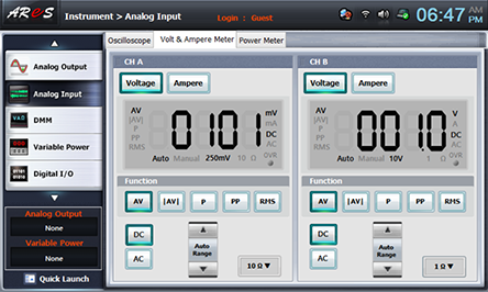
- 1Choose analog input at left menu of Touch LCD panel, choose Volt & Ampere Meter tab and click , , at CH A, CH B.
Locate VR3 in the middle and turn VR2 slowly and adjust so that the value displaye d at CH A(voltage applied to R6) becomes 0.1V(100mV).
- 2Choose dmm at left menu of Touch LCD panel and click .
Turn slowly and adjust VR3 so that the value indicated at DMM(voltage between collector-emitter of TR1) becomes 1V.
- 3Choose analog input at left menu of Touch LCD panel and record the measured value of CH B at Volt & Ampere Meter in the relevant column of table 7-10.
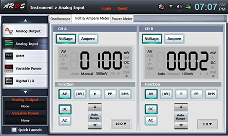
- 4Choose dmm at left menu of Touch LCD panel, turn VR3 slowly to adjust as the voltage between collector-emitter of TR1 given in table 7-10.
Choose analog input at left menu of Touch LCD panel and record the measured value of CH B at Volt & Ampere Meter in the relevant column of table 7-10.
Repeat these processes.
- 5Turn slowly and adjust VR2 so that the value indicated at CH A(the voltage applied to R6) becomes 0.2V(200mV).
Repeat the processes 2), 3), 4) above to measure and record the result in table 7-10.
Experiment of PNP Emitter Earthing Characteristic
1. Using Block c of M07 board, make a connection as in fig.7-28.
- Execute the process of <Experiment of NPN emitter earthing characteristic>
One thing to be noteworthy is that the polarities of powers given to VCC of NPN circuit and PNP circuit are opposite.
2. Record the experiment result in the relevant column of table7-11.
Wiring Diagram
flash
Experiment Result Report
1. Experiment Result Table
Record by calculating as 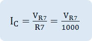
2. Review and Explanation
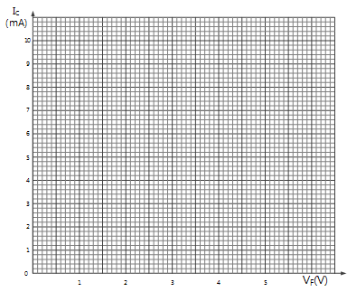
1) Draw the characteristic curve of IC-VCE using table 7-10, 7-11.
(NPN : Blue, PNP : Black)
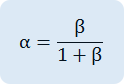
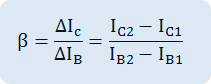
2) From the graph above, choose two curves from the fixed VCE(upper part of 4V) value and calculate the value of β according to the formula.
3) Calculate α by the formula with the calculated β