


PART7Basic Circuit of Semiconductor
Experiment 2 :Rectification Circuit
Theory
Generally, a rectification circuit is the circuit that converts AC to DC. This is the circuit to make either + voltage or – voltage flow within the AC power which has positive(+) voltage and negative(–) voltage successively. The diode has the characteristic to make the current flow to one direction only so is used as the fundamental element for the rectification circuit which changes AC voltage to DC voltage. The types of rectification circuit are half-wave, full-wave and bridge rectification circuits.
① Half-wave Rectification Circuit
Half-wave rectification circuit, the simplest rectification circuit using the diode, has AC input power of single phase, and its diode rectifier is composed of one diode D, and the load is the resistance R. When AC voltage is applied, the period of + is conducted ans the period of – is cut off so it has the waveform of +.
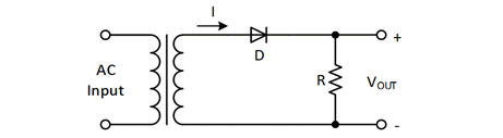
(a) Half-wave rectification circuit

(b) Input/Output wave form Fig. 7-5Half-wave Rectification Circuit and Input/Output Waveform
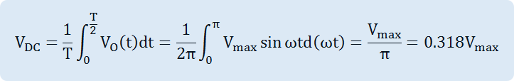
When AC voltage V(t)=Vm sinωt is applied in the circuit as in fig.7-5(a), fig.7-5(b) shows the comparision between input and output waveforms. The average of half-wave output voltage is the value that DC voltmeter indicates. The calculation of this is as below.
Also, the frequency and maximum value of output voltage is same as those of input voltage.
The efficiency of a single phase half-wave rectification circuit is low so this circuit is hard to be used for making high capacity circuit due to big capacity of Trans and semiconductor, and is used in the circuit of small capacity.
Ex) Calculate DC output voltage(VDC) and the current(IDC) flowing through the resistnace when the resistance of 100Ω is connected to the half-wave rectification circuit having effective value of 240V. Also, calculate the power consumed at the load.(Vrms=VS)
Solution)
Vmax =Vrms * 1.414
VDC =0.45 * Vs =0.45 * 240=108 V
VDC =0.318 * Vmax =0.318 * (240 * 1.414)=108 V
IDC = VDC / R = 108 / 100 =1.08 A
P=I2 R=1.082 * 100 = 116 W
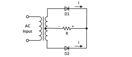
② Full-wave Rectification Circuit
At full-wave rectification circuit, the current flows during whole period of input voltage and at half-wave rectification circuit, the current flows only during half period of the input voltage.
The types of full-wave rectification circuit are the one that using a transformer with a center tap and the one that using a bridge diode.
- Using a Transformer with a Center Tap
As in fig.7-6(a), if a full-wave rectification circuit is composed by using a center tap transformer and two diodes, the diodes D1, D2 are operated in turn during half period of positive(+) and that of negative(-) and the full-wave rectified waveform can be earned at the load side.
(a) Full-wave rectification circuit
(b) Input/Output waveform Fig. 7-6Full-wave Rectification Circuit and Input/Output Waveform
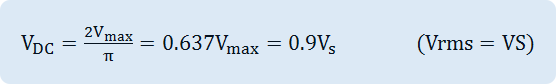
The average value of full-wave rectification is twice bigger than that of half-wave rectification. Also, the frequency of output voltage is double of that of input voltage, and the maximum value of input voltage is same as that of output voltage.
However, to earn the maximum value Vm of actual output voltage, the maximum value of secondary output voltage should be 2Vm.
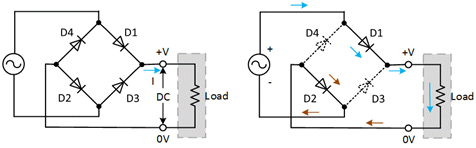
- Bridge Full-wave Rectification Circuit
At bridge diode full-wave rectification circuit, during the positive(+) half period of the power voltage, the diodes D1 and D4 are conducted as fig.7-7(b) and the current flows through the load resistance R, and during the (-) half period, the diodes D2 and D3 are conducted as fig.(c) and the current flows through the load resistance R. The current flows to one direction only during (+) period and (-) period so it is rectified. The average value and frequency of bridge diode full-wave rectification output voltage are same as that of the rectification circuit using a center-tap of transformer.
One difference is that, the power voltage, that is, the secondary voltage of the transformer becomes half than in case of using the center tap, and the size of voltage applied in reverse to nonconducted diode becomes half.
The actual diode is not an ideal diode, so in case of 0.7[V] voltage drop at the diode, the output voltage is indicated as 0.7[V] smaller than the input voltage in case of forward bias. However, in case of bridge diode full-wave rectification, two are conducted at the same time so about 1.4[V] voltage drop occurs.
(a) Bridge rectification circuit (b) Half period of posieive (+)
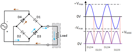
(c) Half period of negative (-) (d) Input/Output waveform
| Average Voltage Vdc | Effective Voltage Vs | Size of Power Voltage | Number of Diode | Reverse Peak Voltage | |
|---|---|---|---|---|---|
| Half-wave Rectification | Vm / π | Vm / 2 | Vm sin ω t | 1 | Vm |
| Full-wave Rectification Using Center Tap |
2Vm / π | Vm √ | 2Vm sin ω t | 2 | 2Vm |
| Full-wave Rectification Using Bridge Diode |
2Vm / π | Vm √2 | Vm sin ω t | 4 | Vm |
Experiment Process
1. Using Block b of M07 board, make a connection as in fig.7-8.
2. Input AC 9V using AC power supply.
3. Connect the load resistance R4, draw one period of AC input waveform in table 7-2 using the oscilloscope, calculate the period, Vpp and frequency and record the result in the table.
4. Observe the output between R4’s both ends with the oscilloscope and draw the result in the relevant column of table 7-2. Calculate and record the average output voltage.
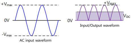
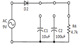
5. Observe and record the output waveform by connecting the capacitor C1 and C2 seperately and describe the difference between connecting the capacitor to the load in parallel and not connecting it.
tab1Experiment 7-2.1 Half-wave Rectification Circuit Experiment
1.Connection(Block b of M07)
1.Circuit Connection
Connect between the right terminal of SW2 of Block b and the right terminal connected to R3 with yellow line.
Connect between the right terminal of L of Block b and upper terminal fo R4 with yellow line.
2.Power Connection
Connect between V1 terminal of Variable Power on M07 board and left terminal of D2 of Block b with red line, and between COM terminal and the earthing terminal with black line.
3.Measuring Instrument Connection
Connect between A+ terminal of Signal Input CH A on front panel and the left terminal of D2 of Block b with red line, and between A- terminal and COM terminal with black line.
Connect between B+ terminal of Signal Input CH B on front panel and the upper terminal of R4 of Block b with red line, and between B- terminal and the earthing terminal with black line.
2.Wiring Diagram
flash
3.Measurement
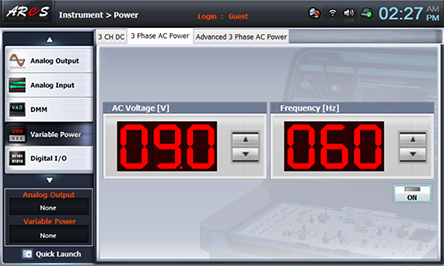
- 1Choose variable power at Touch LCD panel and click 3 Phase AC Power tab.
Click on the right of AC Voltage display and make it as 9.0V.
Click to apply the output of 3 Phase AC Power to the input of Block b.
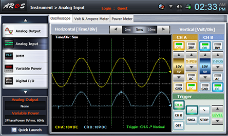
- 2Measure input/output waveforms.
Choose analog input on front panel.
Draw the waeform in oscilloscope screen in the relevant column of table 7-2.
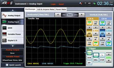
- 3Connecting C1 in Load State and Measuring Output Waveform
Draw the waveform in oscilloscope screen in the relevant column of table 7-2.
- 4Connecting C2 in Load State and Measuring Output Waveform
C2 Connection: Remove the connection between upper terminal and right terminal of C1 of Block b and connect between upper terminal of C2 and right terminal of L with yellow line.
Draw the waveform in oscilloscope screen in the relevant column of table 7-2.
- 5After the measurement, click of 3 Phase AC Power to cut off the output.
Experiment Process
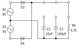
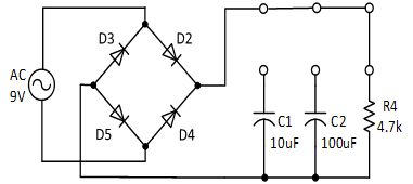
1. Using Block b of M07 board, make a connection as in fig.7-9.
2. Input AC 7V to positive power using AC power supply.
3. Connect the load resistance R4, draw one period of AC input waveform in table 7-3 using the oscilloscope, observe the output between R4’s both ends with the oscilloscope and draw the result in the relevant column of table 7-3. Calculate and record the average output voltage.
4. Observe and record the output waveform by connecting the capacitor C1 and C2 seperately and describe the difference between connecting the capacitor to the load in parallel and not connecting it.
tab2Experiment 7-2.2 Full-wave Rectification Circuit Experiment
1.Connection(Block b of M07)
1.Circuit Connection
Connect between the right terminal of D4 of Block b and the right terminal connected to D2 with yellow line.
Connect between the right terminal of SW2 of Block b and the right terminal connected to R3 with yellow line.
Connect between the right terminal of L of Block b and upper terminal of R4 with yellow line.
2.Power Connection
Connect between V1 terminal of Variable Power on M07 board and left terminal of D2 of Block b with red line, and between V2 terminal and the left terminal of D5 of Block b with red line.
Connect between COM terminal and the earthing terminal with black line.
3.Measuring Instrument Connection
Connect between A+ terminal of Signal Input CH A on front panel and the left terminal of D2 of Block b with red line, and between A- terminal and COM terminal with black line.
Connect between B+ terminal of Signal Input CH B on front panel and the upper terminal of R4 of Block b with red line, and between B- terminal and the earthing terminal with black line.
2.Wiring Diagram
flash
3.Measurement
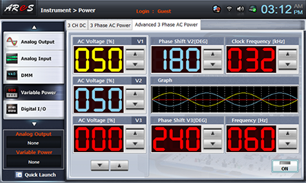
- 1Choose variable power at Touch LCD panel and click Advanced 3 Phase AC Power tab.
Click at the right of AC Voltage[%] V1 display and make it as 50%(7V).
Click at the right of AC Voltage[%] V2 display and make it as 50%(7V).
Set up the phase of Phase Shift V2[DEG] as 180.
Click to output V1, V2 voltages of Advanced3 Phase AC Power.
- 2Measure input/output waveforms.
Choose analog input on front panel.
Draw the waeform in oscilloscope screen in the relevant column of table 7-3.

- 3Connecting C1 in Load State and Measuring Output Waveform
C1 Connection: Connect between upper terminal and right terminal of C1 of Block b with yellow line.
Draw the waveform in oscilloscope screen in the relevant column of table 7-3.
- 4Connecting C2 in Load State and Measuring Output Waveform
C2 Connection: Remove the connection between upper terminal and right terminal of C1 of Block b and connect between upper terminal of C2 and right terminal of L with yellow line.
Draw the waeform in oscilloscope screen in the relevant column of table 7-3.
- 5After the measurement, click of 3 Phase AC Power to cut off the output.
Experiment Process
1. Using Block b of M07 board, make a connection as in fig.7-10.
2. Input AC 9V using AC power supply.
3. Connect the load resistance R4, draw one period of AC input waveform in table 7-4 using the oscilloscope, observe the output between R4’s both ends with the oscilloscope and draw the result in the relevant column of table 7-4. Calculate and record the average output voltage.
4. Observe and record the output waveform by connecting the capacitor C1 and C2 seperately and describe the difference between connecting the capacitor to the load in parallel and not connecting it.
tab3Experiment 7-2.3 Bridge Rectification Circuit Eperiment
1.Connection(Block b of M07)
1.Circuit Connection
Connect between the right terminal of D3 of Block b and its right terminal with yellow line.
Connect between the right terminal of D4 of Block b and its right terminal with yellow line.
Connect between the right terminal of D5 of Block b and its right terminal with yellow line.
Connect between the left terminal of C1 of Block b and its left terminal(earthing terminal) with yellow line.
Connect between the right terminal of SW2 of Block b and its right terminal with yellow line.
Connect between the right terminal of L of Block b and upper terminal of R4 with yellow line.
2.Power Connection
Connect between V1 terminal of Variable Power on M07 board and left terminal of D2 of Block b with red line, and between COM terminal and the left terminal of D5 of Block b with black line.
3.Measuring Instrument Connection
Connect between A+ terminal of Signal Input CH A on front panel and the left terminal of D2 of Block b with red line, and between A- terminal and COM terminal with black line.
Connect between B+ terminal of Signal Input CH B on front panel and the upper terminal of R4 of Block b with red line, and between B- terminal and the earthing terminal with black line.
2.Wiring Diagram
flash
3.Measurement
- 1Choose variable power at Touch LCD panel and click 3 Phase AC Power tab.
Click on the right of AC Voltage display and make it as 9.0V.
Click to apply the output of 3 Phase AC Power to the input of Block b.

- 2Measure input/output waveforms.
Choose analog input on front panel.
Draw the waveform in oscilloscope screen in the relevant column of table 7-4.

- 3Connecting C1 in Load State and Measuring Output Waveform
C1 Connection: Connect between upper terminal and right terminal of C1 of Block b with yellow line.
Draw the waveform in oscilloscope screen in the relevant column of table 7-4.
- 4Connecting C2 in Load State and Measuring Output Waveform
C2 Connection: Remove the connection between upper terminal and right terminal of C1 of Block b and connect between upper terminal of C2 and right terminal of L with yellow line.
Draw the waveform in oscilloscope screen in the relevant column of table 7-4.
- 5After the measurement, click of 3 Phase AC Power to cut off the output.